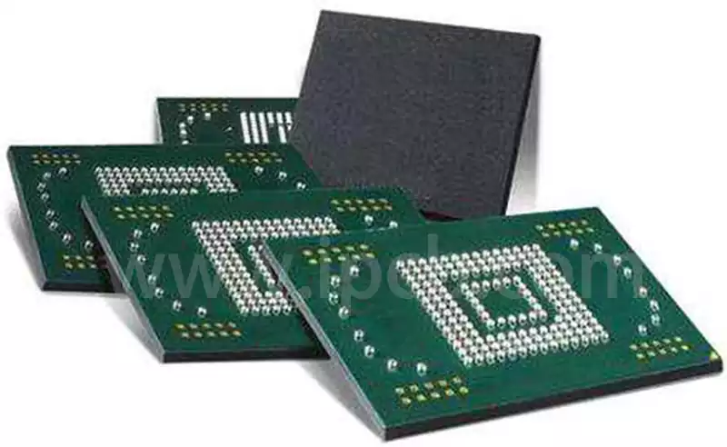
What is FPGA?FPGA board, that is, Field Programmable Gate Array, which is a product of further development on the basis of programmable devices such as PAL, GAL, CPLD, etc. It appears as a semi-custom circuit in the field of Application Specific Integrated Circuits (ASIC). It is as a special integrated circuit (ASIC) in the field of a semi-customized circuits and appeared, both to solve the shortcomings of the custom circuit, but also to overcome the original programmable device gate number of limited shortcomings.
FPGA uses the logic cell array LCA (Logic Cell Array) such a concept, including the internal configurable logic modules CLB ( Configurable Logic Block), input and output modules IOB (Input Output Block) and internal connection (Interconnect) three parts. Field Programmable Gate Array (FPGA) is a programmable device, compared with traditional logic circuits and gate arrays (such as PAL, GAL and CPLD devices), FPGAs have a different structure. FPGAs utilize a small lookup table (16 × 1 RAM) to implement combinational logic, each lookup table is connected to the input of a D flip-flop, which in turn drives other logic circuits or drives I/O, thus constituting both combinational logic and IO.
The logic of the FPGA is realized by loading programmed data into the internal static memory cells, and the values stored in the memory cells determine the logic functions of the logic cells and the connection between the modules or between the modules and the I/O, and ultimately determine the logic functions of the logic cells and the connection between the modules or between the modules and the I/O, and ultimately determine the logic functions of the logic cells. The value stored in the memory cell determines the logic function of the logic unit and the connection between modules or between modules and I/Os, and ultimately determines the functions that can be realized by the FPGA, which allows unlimited programming.
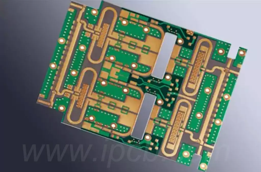
The FPGA hardware is characterized by three key factors: process, gate count, and SERDES rate, and the accompanying EDA software tools are equally important. Comparing FPGA products can start with the technical specifications. From the internal structure of FPGA, it mainly includes: programmable input/output units (I/O), programmable logic blocks (LC), complete clock management (CMT), embedded block RAM (BRAM), cabling resources, embedded underlying functional units and specialized hardware modules.
According to data disclosed by Xilinx, one LUT6 is equivalent to 1.6 LCs, and one LC corresponds to dozens to hundreds of gates, 10 million gates are equivalent to 100,000 LCs, i.e., 100K CLB level FPGAs. unlike ASICs, customers do not only consider the hardware parameters in the purchase of FPGAs, but also the performance of the accompanying EDA software. Unlike ASIC, customers not only consider the hardware parameters but also the performance of the supporting EDA software when purchasing FPGA products. At present, there is a big gap between the high-end products of domestic manufacturers and the high-end products of Xilinx in terms of hardware performance indexes.
Compared with ASIC, FPGA has 3 advantages:
- Editable, more flexible
- Short time-to-market, saving the ASIC wafer cycle
- Avoid one-time engineering costs, and have a cost advantage when the usage is small.
(1) Flexibility: By programming FPGA, FPGA can perform any logic function that ASIC can perform. the unique advantage of FPGA lies in its flexibility, that is, it can change the function of the chip at any time, and in the stage where the technology is not yet mature, this characteristic can reduce the cost and risk of the product, which is especially important in the early stage of 5G.
(2) Time-to-market: Since FPGAs can be used directly after being bought and programmed, FPGA solutions do not need to wait for a three-month to one-year chip flow cycle, thus gaining time-to-market for enterprises.
(3) Cost: FPGA and ASIC main difference in the ASIC program has a fixed cost and FPGA program is almost no, in the use of a small amount of time, FPGA program does not need to pay a one-time million-dollar cost of flow, but also do not have to bear the risk of failure of the flow, the cost of FPGA program is lower than the ASIC, with the increase in the use of the amount of FPGA program in the cost of the advantages gradually shrink, more than a certain amount of use, after the FPGA program, the cost is lower than the ASIC, with the increase of the amount of cost of FPGA program. As the usage volume increases, the cost advantage of FPGA solution gradually shrinks, and after exceeding a certain usage volume, ASIC solution is more advantageous in cost due to the economies of scale generated by a large number of flow chips.
How does FPGA board programming work?
FPGA programming allows you to manipulate the circuitry using HDL based on the functionality you want the device to have.This process is different from programming a GPU or CPU because the program you write will not run sequentially.Instead,you use HDL to create the circuit and physically modify the hardware according to the features you want.
This process is similar to software programming, in which the code you write is converted to a binary file and loaded on the FPGA. But the result is that the HDL physically modifies the hardware, rather than running the software through a tightly optimized device.
A program on the FPGA assembles lower-level electronic components such as logic gates and memory blocks that work together to accomplish a task. Because you are manipulating the hardware from scratch, the FPGA brings a high degree of flexibility. You can adjust basic features such as memory or power consumption to suit the task.
How to Program FPGAs
While FPGA board only exist in the realm of hardware engineers,AI scientists and software programmers can now access new platforms that make the process feel like writing a software program.With the right tools,you’ll find a solution for programming FPGAs that meets your needs at the current level of hardware and software knowledge.
If you are used to programming for GPUs,the process of writing FPGA code will feel very similar,even if the results are a bit different. programming for FPGAs involves writing the code,translating that program into a lower level language as needed,and converting that program into a binary file.You will then provide the program to the FPGA,operating as if you were asking the GPU to read a piece of software written in C++.It’s that simple.
But in order to optimize that programming process, you need access to the right platform.Fortunately AMD has the perfect solution, a groundbreaking set of tools to help software developers at every step of the FPGA programming process.