What is trace width in PCB?PCB Trace width is the width of the wires or alignments on a circuit board.It is usually measured in millimeters or inches, e.g., 0.2mm, 8mil, etc. The choice of line width depends on factors such as the circuit’s power requirements, signal frequency, impedance control and manufacturing process requirements. Depending on current and signal characteristics, larger line widths provide better current carrying capacity and lower resistance, while smaller line widths allow for higher density and finer alignment.
PCB trace width is the width of the conductive path (i.e. copper foil) on the PCB. It directly affects the following aspects:
1.Current carrying capacity: the greater the line width, the greater the current that can pass. Too small a line width may lead to too high a current density, causing heat, increased resistance and even line burnout.
2.Signal transmission quality: for high-speed digital signals or high-frequency analog signals, the line width affects the signal transmission speed, impedance matching and crosstalk and other characteristics, directly affecting the stability and accuracy of the circuit.
3.Manufacturing difficulty and cost: too fine a line width will increase the production difficulty, may require more sophisticated processes and higher process requirements, thereby increasing costs; conversely, too wide a line width may be a waste of materials, also not conducive to cost control.
PCB line width should follow the following basic principles:
1.Meet the current requirements:First, according to the expected maximum current value in the circuit, with reference to the thickness of the copper foil, temperature rise allowable range and other factors, the use of the formula to calculate the minimum line width required. Usually, this requires reference to industry standards such as IPC-2221 or the use of specialized current carrying capacity calculation tools.
2.Comply with signal integrity requirements:For high-speed or high-frequency signal lines, the line width should be calculated in accordance with impedance matching theory based on factors such as transmission rate, signal type, and transmission distance in order to minimize reflections, crosstalk, and other problems. If necessary, specific topology (e.g. microstrip line, ribbon line) and termination technology may also be required.
3.Take into account the production process:Consider the manufacturer’s minimum line width and line spacing capabilities, as well as Design Rule Check (DRC) requirements. In general, High-Density Interconnect (HDI) boards may require finer trace widths, while common multilayer boards have less stringent line width requirements. Economic considerations:In order to meet the functional requirements of the premise, the choice of both guaranteed performance and reasonable economic line widths, to avoid the cost of excessive design waste.
Determine the common PCB circuit board line width considerations Select the appropriate PCB line width, need to consider the following aspects:
1.current demand: according to the actual current load of each part of the circuit design,with reference to the relevant specifications (such as IPC-2221 standard) to calculate the minimum trace width required to ensure that the line can safely and effectively conduct current.
2.Signal speed and impedance matching:For high-speed signal lines,the trace width should be determined by the impedance calculation tool based on the target impedance value (usually 50Ω or 75Ω) and the dielectric constant of the plates used. At the same time, the spacing between neighboring wires should also be considered to control crosstalk.
3.Design rules and manufacturing processes:Different manufacturers have different process capabilities and generally have their own specific minimum/maximum pcb line width limits.The design should follow the Design Rule Check (DRC) provided by the manufacturer to ensure the manufacturability of the design.
4.Overall layout and space utilization: Under the premise of meeting the above electrical requirements, the line width should also take into account the overall layout of the PCB and size limitations, reasonable use of space, optimize wiring density.
Signal lines that need to be made impedance should be set in strict accordance with the trace width and line spacing calculated by stacking layers. For example, RF signals (conventional 50R control), important single-ended 50R,differential 90R,differential 100R and other signal lines,through the stacked layer can be calculated by the specific line width and line spacing
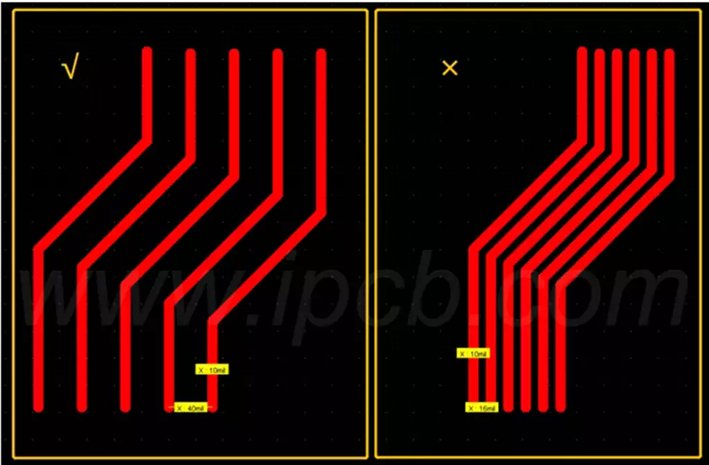
The design of the trace width line spacing should take into account the production process capabilities of the selected printed circuit board production plant,such as if the design set the line width line spacing more than the cooperation of the PCB manufacturer’s process capabilities, light need to add unnecessary production costs, or lead to the design can not be produced. In general, under normal circumstances, the line width and line spacing control to 6/6mil, 12mil over the hole selection (0.3mm), more than 80% of the basic PCB manufacturers can produce, the production of the lowest cost. Line width and pitch control to a minimum of 4/4mil, over-hole selection 8mil (0.2mm), the basic 70% of PCB manufacturers can produce, but the price is slightly more expensive than the first case, not too expensive. Line width and spacing of the minimum control to 3.5/3.5mil, over the hole selection 8mil (0.2mm), this time there are some PCB manufacturers can not produce, the price will be more expensive. Line width and line spacing control to a minimum of 2/2mil, over the hole selection of 4mil (0.1mm, at this time is generally HDI blind buried hole design, need to hit the laser over the hole), at this time most of the PCB manufacturers can not produce, the price is the most expensive. Here the line width line spacing when setting rules, refers to the line to the hole, line to the line, line to the pad, line to the hole, hole to the disk and other elements between the size. Setting rules consider the design bottleneck in the design file. If there is a 1mm BGA chip, the pin depth is shallow, between the two rows of pins only need to walk a signal line, can be set 6/6mil, the pin depth is deeper, between the two rows of pins need to walk 2 signal lines, it is set to 4/4mil; there is a 0.65mm BGA chip, generally set to 4/4mil; there is a 0.5mm BGA chip, the general width of the line spacing must be set to a minimum of 3.5/3.5mil; 0.4mm BGA chip, generally need to do HDI design. Generally for the design of bottlenecks, you can set up regional rules, local trace width and line spacing set a small point, the rest of the PCB rules to set up a larger number in order to produce, improve the production out of the PCB pass rate.
PCB circuit boards commonly used pcb line width is not a fixed value, but based on specific application scenarios flexible adjustment. In general, the common line width range is roughly as follows:
- General digital circuits: for low-speed, low-power digital circuits, the trace width is usually between 8 mil (about 0.2mm) and 16 mil (about 0.4mm). This range meets most current requirements and is easy to manufacture.
- High-speed signal lines: For applications such as high-speed data transmission, high-frequency circuits, etc., the line width may need to be finely designed according to the target impedance, with common values between 4mil (~0.1mm) and 10mil (~0.25mm).
- Power and Ground Lines: In order to provide sufficient current carrying capacity and good noise immunity, the line width of power and ground lines is usually wider than that of signal lines, sometimes up to 20mil (about 0.5mm) or more.
- Special applications: for micro-fine pitch packaging devices, high-density interconnect (HDI) boards and other special applications, the line width may need to be further reduced, and even up to 2mil (about 0.05mm) or less, which usually requires the use of advanced laser direct imaging (Laser Direct Imaging, LDI) and other process technologies.
PCB trace width design is a critical part of circuit design, which needs to find the best balance between current carrying capacity, signal quality, manufacturing difficulty and cost. By taking into account the specific needs of the circuit, signal characteristics, and manufacturing capabilities, we can design a PCB that meets functional requirements and is economical.