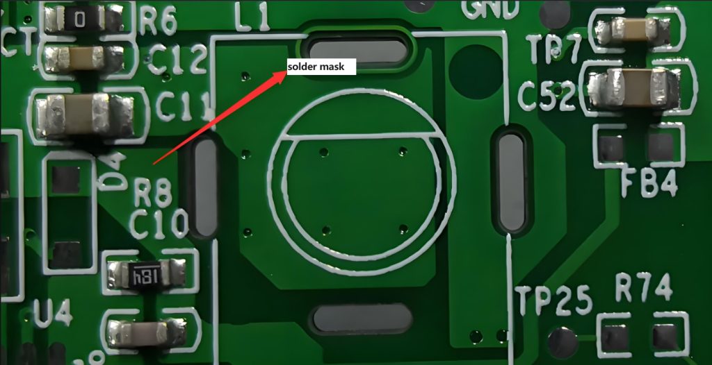
Solder mask in pcb, is also called PCB solder mask film in flexible circuit boards, using green, yellow, red, black, blue and other photosensitive inks sprayed on the surface of the PCB circuit board.Solder Mask is a protective layer applied to the surface of a circuit board that prevents short circuits from occurring when other circuit parts on the board are soldered to the solder paste, and protects the circuit surface from corrosion and contamination. In the manufacture of PCBs, soldermask is usually applied after etching, creating a screen-print-like appearance.
It is applied to areas of the circuit board that do not require solder paste soldering, exposing only the locations where soldering is required,and also protecting the board from environmental influences.It prevents short circuits from non-metallic free contaminants,protects the board surface from Scratch damage, enhances the board’s heat resistance, and improves the signal integrity and electrical performance of the board.
Why do PCB circuit board solder mask?
In the printed circuit board (PCB) manufacturing process, the coating of solder mask ink is a very critical process. Both sides of the PCB substrates are copper layers, and the PCB plateboard without solder mask is easy to be oxidized when exposed to the air,and becomes a defective product, which also affects the electrical performance of the PCB board.Therefore, there must be a protective coating on the surface of the PCB circuit board that can prevent the oxidation reaction between the PCB and the air,and this coating is the solder mask layer covered with solder mask paint material.Therefore, the part of the PCB that is covered by ink refers to the solder mask in pcb.
1. Prevent short circuit: The solder mask can cover the area between the wire and the pad, reducing the risk of short circuit. There are many wires and pads present on the PCB board, which can lead to short circuits if not properly isolated. The solder mask provides the necessary isolation, ensuring the stability and correct functioning of the circuit.
2. Prevent leakage and electrical interference: The solder mask in pcb provides electrical insulation, reducing the possibility of leakage and electrical interference. On circuit boards, if there is no proper isolation between wires or pads, it can lead to interference and leakage of electrical signals. Solder masks help reduce this and protect circuit components from the external environment.
3. Protect circuit components: The solder mask layer can provide a layer of protection to prevent the components on the surface of the PCB from being eroded or damaged by the external environment (such as dust, moisture, etc.). This helps to improve the reliability and longevity of the circuit.
4. Improve the quality of soldering: The presence of a solder mask can limit the diffusion of solder, making soldering more precise and controllable. The soldering pads on the pads and component pins are protected by the solder mask and are not easily disturbed by external factors, thus improving the soldering quality.
5. Convenient maintenance and debugging: The presence of solder mask can provide clear circuit structure information, which is helpful for maintenance and debugging work. With solder masks, technicians can more easily identify circuit paths and connections, reducing errors and time.
Types of solder mask in pcb
According to the different welding processes, solder mask can be divided into 3 types.
1. Spot welding: The weldment is pressed between the two columnar electrodes, and the weldment is heated by electricity to melt at the contact to form a nugget, and then the power is cut off, and it solidifies and crystallizes under pressure to form a dense solder joint. Spot welding is suitable for welding thin plates (laps) and steel bars below 4 mm, and is widely used in the production of automobiles, aircraft, electronics, instruments and daily necessities.
2. Seam welding: Seam welding is similar to spot welding, except that a rotating disc electrode is used instead of a cylindrical electrode. The superimposed workpieces are pressurized and energized between the discs and fed in with the rotation of the discs to form a continuous weld. Seam welding is suitable for welding thin plate lap joints with a thickness of less than 3 mm, and is mainly used in the production of hermetically sealed containers and pipes.
3. Butt welding: Butt welding can be divided into resistance butt welding and flash butt welding.
(1) Resistance butt welding
The welding process is to first apply the top forging pressure (10~15 MPa) to make the workpiece joint close contact, energized and heated to a plastic state, and then apply the top forging pressure (30~50 MPa), and at the same time cut off the power, so that the weldment contact is welded with plastic deformation under pressure. Resistance butt welding is easy to operate, and the joint shape is smooth, but the requirements for processing and cleaning the end face of the weldment are high, otherwise it will cause uneven heating of the contact surface, produce defects such as oxide inclusion, and impermeable welding, and affect the welding quality. Therefore, resistance butt welding is generally only used for welding workpieces with a diameter of less than 20 mm, a simple cross-section, and a small force.
(2) Flash butt welding
The welding process is to first energize, and then make the two weldments slightly contact, due to the uneven surface of the weldment, so that the current density of the contact point is very large, the metal quickly melts, gases, blasts, splashes out of sparks, resulting in flash phenomenon. Continue to move the weldment, produce new contact points, flash phenomenon continues to occur, when the end face of the two weldments is all melted, quickly pressurized, then the power is cut off and continue to pressurize, so that the weldment is welded. The joint quality of flash butt welding is good, and the pre-welding cleaning of the joint surface is not high. It is often used to weld important workpieces with large forces. Flash butt welding can not only weld the same metal, but also weld dissimilar metals such as aluminum steel, aluminum and copper, and can weld 0.01 mm wire, 500 mm diameter pipes and 20 000 mm2 plates.
If the treatment is not improper, the solder mask will have defects such as uneven solder mask, false copper exposure, substrate bruising, and broken wire, so it is necessary to pay attention to the operation points when dealing with the solder mask.
Flow of solder resist process
Solder Resist Film Negative→Punching Negative Positioning Hole→Cleaning Printing Board→Making Ink→Double-Sided Printing→Pre-Baking→Exposure→Development→Heat-Setting
Principle of Solder Resist Exposure
Exposure is the core of the entire solder resist process, the principle of solder resist exposure is mainly the use of light scattering and the photopolymer contained in the solder resist film to produce an optical reaction, so as to achieve the desired effect.
Exposure in the soldermask process is very critical, when the exposure is excessive, due to the scattering of light, graphics or lines of the edge of the soldermask film and the reaction of light to generate a residual film, which reduces the degree of resolution, resulting in the development of graphics smaller, thinner lines; if the exposure is insufficient, the result is the opposite of the above, the development of graphics become larger, thicker lines.
If the exposure time is long, the measured line width is negative tolerance; exposure time is short, the measured line width is positive tolerance. In the actual process, available “light energy integrator” or “exposure ruler” to determine the optimal exposure time.
Selection of exposure light source
Exposure light source characteristics directly affect the solder resist exposure quality and efficiency, the spectrum emitted by the light source should be matched with the absorption spectrum of light-sensitive materials in order to obtain a better exposure.
Currently solder resist ink absorption wavelength of 350 ~ 450nm, shorter wavelength light, after exposure imaging graphics edge neat and clear, longer wavelength light energy penetration is good, can make the ink deep and fast curing. Due to the wavelength below 300 nm is easy to be absorbed by the glass and the polyester base of the substrate, so the light source selected in the exposure machine and its wavelength is generally between 310 ~ 440nm.
Solder mask in pcb plays an important role and efficacy in the electronics manufacturing industry, ensuring the reliability and stability of the circuit by preventing short circuits, leakage and electrical interference, improving soldering quality, and facilitating maintenance and debugging. It is believed that with the progress of science and technology, solder mask will play more roles and effects in the future and contribute greater value to the electronics manufacturing industry.