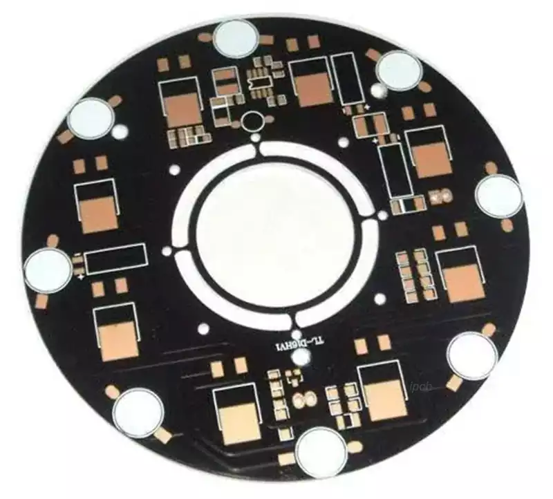
Within electronic products, PCBs, though fundamental components, directly impact the performance and reliability of the entire device. Many engineers observing design evaluations note a consistent pattern: switching from conventional FR-4 PCBs to ceramic PCBs typically results in a significant increase in overall costs, sometimes even multiplying them several times over. This price disparity stems not from simple manufacturer pricing strategies, but from the inherent characteristics of ceramic PCBs in terms of material composition, manufacturing processes, and application positioning. To truly comprehend this cost difference, one must analyse the realities at the manufacturing level.
Different materials mean different cost starting points
The widespread adoption of ceramic materials in high-power and high-reliability electronics stems from their exceptional high-temperature resistance, superior thermal conductivity, and long-term electrical and structural stability. However, these performance advantages come at a cost. Firstly, ceramic substrates demand extremely high purity and formulation consistency in raw materials. The screening, refinement, and quality control of these materials inherently entail higher manufacturing costs. Secondly, ceramic substrates undergo multiple complex processes including forming, degreasing, and high-temperature sintering. These procedures demand strict control over temperature profiles and atmospheres, resulting in significantly higher overall energy consumption compared to conventional PCB material preparation. Furthermore, the number of suppliers capable of consistently delivering high-quality ceramic substrates remains relatively limited, with insufficient market competition further restricting cost optimisation potential. Considering these factors collectively, even disregarding subsequent processing, the cost of ceramic PCBs is markedly higher than that of conventional PCBs from the substrate stage onwards.
The manufacturing process is more complex and presents greater challenges.
In practical applications, ceramic PCBs are often simplistically understood as ‘replacing the substrate of traditional PCBs with ceramic’. However, from a manufacturing perspective, the underlying process logic of these two product types differs fundamentally. Conventional PCBs rely on mature processes such as lamination, electroplating, and etching. Their highly standardised and stable process systems, honed through years of mass production, have developed considerable tolerance for manufacturing variations. Ceramic PCBs, however, predominantly utilise specialised techniques like DBC (Direct Bonded Copper), AMB (Advanced Multilayer Bonding), and thick/thin film processes. These often require execution under high-temperature conditions or in controlled atmospheres, imposing stricter demands on process parameters.
During actual manufacturing, ceramic PCBs exhibit extreme sensitivity to temperature profiles, atmosphere composition, and thermal stress matching between materials. Even minor deviations can trigger delamination, cracking, or bonding failures. Furthermore, critical processes are often irreversible; defects occurring during sintering or bonding stages render products virtually irreparable through rework, necessitating scrapping. Moreover, the operational window for such processes is narrow, heavily reliant on engineering expertise and accumulated process knowledge. Achieving stable mass production itself represents a significant technical challenge. Consequently, compared to conventional PCBs with mature processes and higher fault tolerance, the increased manufacturing difficulty and risk associated with ceramic PCBs directly translate into higher production costs.
Significant capital expenditure, yet typically low output
Ceramic PCB production necessitates specialised equipment such as high-temperature sintering furnaces, vacuum bonding apparatus, and laser processing systems. Such machinery demands substantial investment and maintenance costs while offering limited versatility. In practice, ceramic PCBs are predominantly employed in specialised fields like power modules and automotive electronics, where orders often involve small batches and multiple specifications. The capital investment cannot be rapidly amortised through large-scale shipments, ultimately manifesting as higher per-unit costs.
Processing yields remain low, heightening manufacturing risks
Compared to resin-based substrates, ceramic materials exhibit high hardness and poor ductility, elevating failure risks during processing. Operations like cutting, drilling, chamfering, and heat treatment render ceramic substrates prone to micro-cracks, edge chipping, or internal latent defects. These issues often remain undetectable during visual inspection yet compromise subsequent reliability. Even under conditions of relatively mature process parameters and high equipment precision, the overall processing yield of ceramic PCBs typically struggles to match that of conventional PCBs.
More challenging still, certain defects do not manifest immediately during front-end processes but gradually emerge during subsequent electrical performance testing, thermal cycling tests, or even in actual application. Should issues arise at these stages, the costs already invested in ceramic substrates, processing fees, labour, and energy consumption cannot be recovered, necessitating scrapping. Such latent risks statistically inflate the average manufacturing cost per qualified unit, constituting a key factor in the greater difficulty of cost control for ceramic PCBs compared to conventional PCBs.
Design and engineering support costs are more concentrated
Ceramic PCBs are typically employed in high-power, high-reliability applications, demanding greater sophistication during the design phase. Aspects such as thermal path design, thermal stress control, and soldering/packaging compatibility require extensive engineering validation.
These investments are often spread across large-volume projects for standard PCBs, whereas ceramic PCB projects concentrate these costs within limited production runs, making them appear more ‘pronounced’.
The higher cost of ceramic PCBs stems not from a single factor, but from the combined influence of material properties, manufacturing processes, equipment investment, processing yield rates, and engineering support. The decision to adopt ceramic PCBs hinges not on whether they are ‘expensive,’ but on whether they genuinely align with the product’s performance requirements and application context.