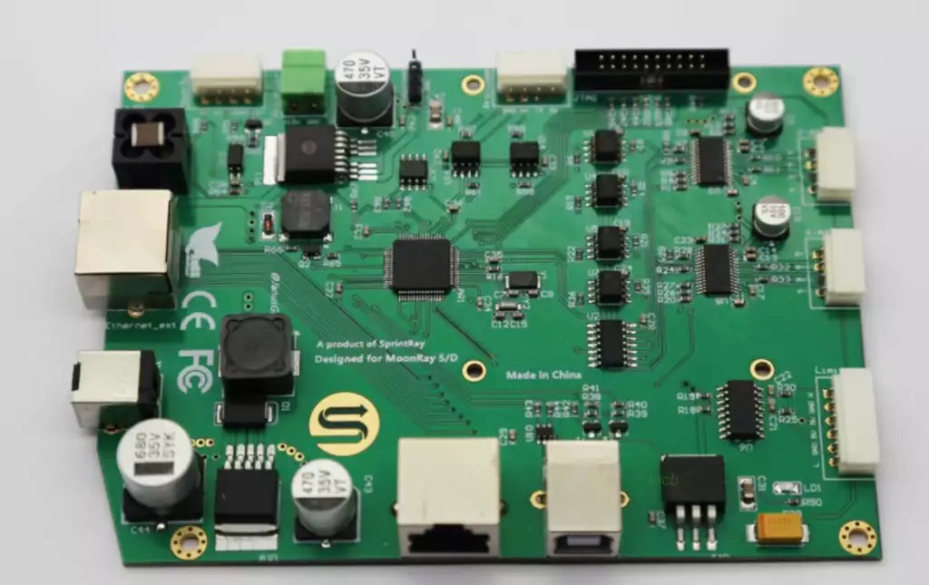
An 8-layer pcb features one circuit layer on each of the top and bottom surfaces, with six intermediate ground and power planes. This structure enhances the board’s stability and reliability while significantly reducing electromagnetic noise and interference. In practical applications, 8-layer pcbs are primarily employed for high-speed signal transmission and complex circuit designs.
An 8-layer PCB is a multilayer circuit board formed by bonding eight mutually insulated conductive layers (such as copper foil) using adhesive materials (e.g., epoxy resin). Electrical connections between layers are achieved via vias, forming a complete circuit system. Its design objective is to provide optimised signal transmission paths and power distribution solutions for high-speed, high-density, and high-reliability electronic equipment.
When designing the layer distribution for an 8-layer PCB, the following aspects require consideration:
- Distribution of Signal and Power Layers
To ensure stable and reliable signal transmission, signal and power layers must be distributed across different layers in an 8-layer PCB. Typically, inner layers 3 and 4 serve as ground planes, inner layers 5 and 6 as power planes, while inner layers 1 and 2 alongside outer layers 7 and 8 function as signal planes. - Ground plane distribution
Multiple ground planes should be distributed within the ground layer of the 8-layer pcb, positioned as close as possible to signal or power planes. This effectively minimises electromagnetic noise and interference. - Impedance Matching
In high-speed data transmission 8-layer pcb designs, signal transmission must meet impedance matching requirements. Within the distributed layers of the PCB eight-layer board, signal trace widths and spacing must be adjusted according to design specifications to ensure impedance matching. - Use of Fillers
To mitigate electromagnetic noise and interference in 8-layer PCB designs, fillers may be incorporated within the distribution layers. These fillers effectively reduce electromagnetic noise while enhancing the PCB’s mechanical strength and thermal conductivity.
Common laminate structures for 8-layer pcb
Scheme One
Signal 1 layer: Located on the component side, serving as a microstrip trace layer.
Signal 2 layer: Positioned internally, functioning as a microstrip trace layer. This layer offers superior routing characteristics (particularly advantageous for routing along the X-axis).
Ground layer: Ground plane.
Signal 3 Layer: A stripline routing layer with favourable routing characteristics.
Signal 4 Layer: Also a stripline routing layer.
Power Layer: The power supply layer.
Signal 5 layer: Internal microstrip trace layer.
Signal 6 layer: Microstrip trace layer.
This scheme employs an alternating arrangement of signal and power planes. However, it fails to fully leverage the electromagnetic shielding properties inherent in a multilayer structure. Consequently, its electromagnetic absorption capability is inadequate, and the power impedance is relatively high.
Scheme Two
Signal 1 Layer: On the component side, serves as a microstrip trace layer, providing an excellent routing layer.
Ground Layer: Ground plane, offering good electromagnetic wave absorption capability.
Signal 2 Layer: Stripline trace layer, delivering good routing performance.
Power Layer: Power plane, forming an effective electromagnetic absorption structure in conjunction with the underlying ground plane.
Ground Layer: Ground plane, exhibiting good electromagnetic wave absorption capability.
Signal 3 Layer: A stripline routing layer with excellent routing performance.
Ground Layer: Ground plane with good electromagnetic wave absorption capability.
Signal 4 Layer: A microstrip routing layer with satisfactory routing performance.
This scheme is regarded as the optimal stackup configuration. By employing multiple ground reference planes, it delivers exceptional electromagnetic absorption capability, robustly safeguarding signal stability and integrity.
Scheme Three
Signal 1 Layer: Located on the component side, serving as a microstrip trace layer with excellent routing properties.
Ground Layer: Ground plane with good electromagnetic wave absorption capability.
Signal 2 Layer: Stripline trace layer with favourable routing characteristics.
Power Layer: Power plane, forming an effective electromagnetic absorption structure in conjunction with the underlying ground plane.
Signal 3 Layer: A stripline routing layer with favourable routing characteristics.
Power Layer: A power plane exhibiting significant power impedance.
Signal 4 Layer: A microstrip routing layer delivering satisfactory routing performance.
As a variant of Solution One, this approach enhances electromagnetic interference (EMI) performance by incorporating a reference plane, enabling more effective control of signal layer characteristic impedance. However, further optimisation of the power plane layout remains necessary.
Core Advantages of the 8-Layer PCB
Signal Integrity Enhancement: Alternating dedicated signal layers with ground plane layers reduces signal interference by up to 60%, supports 56Gbps high-speed transmission, and decreases timing jitter by 40%.
Enhanced Electromagnetic Compatibility: With complete ground plane coverage exceeding 85%, electromagnetic radiation is reduced by 12-15dB, making it suitable for high-frequency, high-power applications.
Thermal Optimisation: Multi-layer structures combined with heat-dissipating via arrays reduce chip junction temperatures by 18°C, suitable for high-power devices.
High Space Utilisation: Maintains performance while saving approximately 70% space compared to 6-layer boards, ideal for compact designs.
8-Layer PCB Applications
High-Frequency, High-Speed Scenarios: Such as communication base stations and radar systems requiring low latency and high stability.
High-density integration: Consumer electronics demanding stringent space constraints and signal integrity, such as smartphones and AR/VR devices.
High-power equipment: Applications requiring high current handling and electromagnetic shielding, including medical instruments and power electronics.
Limitations
Increased cost: Complex manufacturing processes may elevate costs by 30%-50% compared to 6-layer boards.
Design complexity: Specialised tools and expertise are required; standard designs struggle to balance signal integrity and thermal management demands.
8-layer PCB offers distinct advantages. Despite cost and design challenges, their application prospects remain promising, continuing to drive the advancement of electronic devices towards higher performance and miniaturisation.