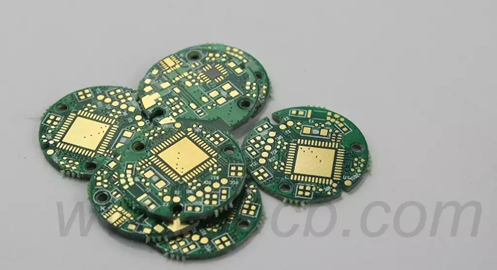
Circuit boards are a critical component in modern electronic products, and HDI boards and FR-4 circuit boards are two common circuit substrate materials used in the electronics industry. Although they both have unique advantages and application scenarios, there are significant differences in performance, manufacturing processes and areas of application.
- Material Composition
HDI circuit boards mainly use high-density interconnect technology, and their substrates are usually polyimide or other high-performance materials. These materials are able to meet the needs of high-frequency performance and high reliability.
FR-4 circuit boards, on the other hand, are made of epoxy resin and electronic-grade glass cloth as the main materials through the press-fit process.FR-4 materials are widely used for their good insulation and mechanical strength, and are suitable for manufacturing simple circuit applications. - Performance
In terms of performance, HDI boards offer higher interconnect density and better signal integrity for high-end electronics such as smartphones and tablets. This allows HDI boards to excel in high frequency, high speed circuits with less signal loss.
Comparatively, FR-4 boards, while stable in general applications, are relatively weak in signaling performance and high-frequency characteristics, making them suitable for use in the manufacture of simple electronic devices such as televisions and audio equipment.
- Cost and applicability
HDI circuit boards are more expensive to manufacture, but for boards with a density of more than eight layers, the use of HDI technology can reduce the overall cost of manufacturing, compared with the traditional multilayer circuit board manufacturing technology is more economical. However, due to its complex manufacturing process, HDI boards are typically used in high-end electronics.
FR-4 circuit boards are less expensive to produce, are suitable for mass production, and are widely used in most economical products. Especially in electronic devices that do not require high-density interconnections, FR-4 boards are also standard materials.
- Application Scenarios
HDI circuit boards are widely used in areas with high performance requirements, such as smart phones, laptops, and automotive electronics. These applications require high-density and high-reliability circuit solutions.
FR-4 circuit boards, on the other hand, are suitable for relatively simple electronic products, such as home appliances, TVs and audio equipment, to meet the basic performance requirements of these products.
The high density of HDI pcb has five main features in its design:
- The board contains blind holes and other micro-conductor hole design;.
- Hole diameter of 152.4um or less, and the hole ring in the 254um or less.
- Density of soldered joints is greater than 50cm/cm2.
- The density of wiring is more than 46 cm/cm2.
- The width and distance of the line does not exceed 76.2um.
HDI board densification is mainly embodied in the hole, line, interlayer thickness of three major aspects.
- Through-hole miniaturization. Its main manifestation is the aperture of less than 150um microporous pore technology and cost, production efficiency, and precision control of holes and other aspects of the high demand.
- Refinement of line width and line distance. Its main performance in the wire defects and wire surface roughness requirements are becoming more and more stringent.
- Thin dielectric thickness. It is mainly manifested in the interlayer media thickness to 80um and the following trend, and the thickness uniformity requirements are becoming more and more stringent, especially for the characteristic impedance control of high-density boards and packaging substrates.
FR4 boards process:
- single panel process flow:
Under the material grinding → drilling → outer graphics → (full-board gold-plated) → etching → inspection → silkscreen solder resist → (hot air leveling) → silkscreen characters → shape processing → test → inspection - Double-sided tin spraying board process flow:
Grinding of material → drilling → copper thickening → outer graphics → tin plating, etching and retinning → secondary drilling → inspection → silk screen solder resist → gold-plated plug → hot air leveling → silk screen characters → shape processing → test → inspection | … - Multilayer board tin spraying board process flow:
Grinding of material → drilling positioning holes → inner layer graphics → inner layer etching → inspection → blackening → lamination → drilling → copper thickening → outer layer graphics → tin plating, etching and de-tinning → secondary drilling → inspection → silk-screen solder resist → gold-plated plug → hot air leveling → silk-screen characters → shape processing → test → inspection - Multilayer plate nickel gold plating process:
Grinding the edge of the material → drilling positioning holes → Inner layer graphics → Inner layer etching → inspection → blackening → lamination → drilling → immersion copper thickening → outer layer graphics → gold plating, de-epitaxialization etching → secondary drilling → Inspection → silk screen solder resist → silk screen characters → shape processing → test → inspection - Multilayer plate immersion nickel gold plate process flow:
Grinding the edge of the material → drilling positioning holes → Inner layer graphics → Inner layer etching → inspection → blackening → lamination → drilling → copper thickening → outer layer graphics → Tin-plating, etching and retinning → Secondary drilling → Inspection → silk screen solder resist → chemical immersion of nickel gold → silk screen characters → shape processing → test → inspection
HDI circuit board production process mainly includes the following steps:
- Design: First, according to the schematic diagram of the circuit, the design of the PCB board is carried out.
- Plate making: Use CAM software to integrate the designed circuit board diagram into a Gerber file and make a light board on the substrate of the circut board.
- Inner layer manufacturing: The circuit diagram made by the optical board is molded on the substrate to form the desired line.
- Film forming: Chemical copper plating or copper plating is performed on the surface of the PCB to form a copper foil layer.
- Laser Drilling: Drill holes in the copper foil layer with a laser.
- Outer layer manufacturing: the board is pressed onto the chemically coated copper foil layer to form the outer circuit.
- Windowing: The outer hdi boards are windowed for soldering components through photolithography and etching processes.
- Surface treatment: Chemical treatment of the finished circuit boards to turn the surface into something like a solder alloy.
- Rust prevention treatment: Rust prevention treatment such as spraying on the circuit board to improve its service life.
Differences in Manufacturing Processes for HDI and FR4 Boards
In terms of manufacturing process, there are significant differences between HDI (High Density Interconnect) boards and FR4 boards, mainly in terms of the number of layers, aperture and production process. These differences make them very different in application scenarios and performance.
Differences in Layer Count
HDI boards typically have a higher number of layers, which allows them to realize more complex circuit designs in a limited space. HDI boards are designed with blind and buried vias to make connections between layers, and are suitable for high-density applications such as smartphones and other portable electronic devices. In contrast, FR4 boards are usually single-sided, double-sided, or multilayer structures with relatively few layers for general-purpose electronics .
Variation in aperture size
In terms of aperture size, HDI boards use laser drilling technology to achieve smaller apertures down to 0.1 mm. This tiny aperture improves the wiring density and performance of circuits and is suitable for complex circuit requirements. FR4 circuit boards, on the other hand, are mainly mechanically drilled, with a minimum aperture generally not less than 0.15 mm, and their design complexity and wiring density are relatively low .
Manufacturing Process Complexity
HDI boards require the use of more advanced manufacturing techniques, including laser drilling and more complex pattern transfer processes. While these techniques can provide higher circuit performance and density, they also correspondingly increase production costs and time. FR4 boards are relatively simple to manufacture, often including traditional etching, printing and drilling steps, and are suitable for mass production, resulting in lower costs and shorter production cycles.
Differences in Material Selection
HDI boards are more diverse in material selection, and materials with higher Tg values (glass transition temperature) are often chosen to meet the thermal stability needs of high-density multilayer circuits. Common materials include BT resins and other high-performance composites. While FR4 circuit boards generally use materials such as glass fiber reinforced epoxy resin, which has good mechanical properties and cost-effective .
There are significant differences in the manufacturing processes between HDI and FR4 boards, including the number of layers, apertures, production complexity, and material selection. These differences determine that HDI boards are suitable for high-density, high-performance electronic products, while FR4 circuit boards are more suitable for general use and have a higher cost performance. When selecting a circuit board, a reasonable decision should be made based on specific application needs and technical requirements.