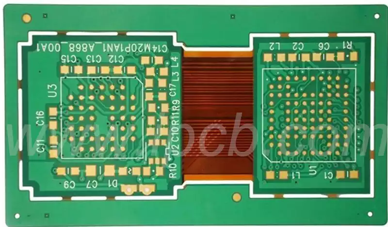
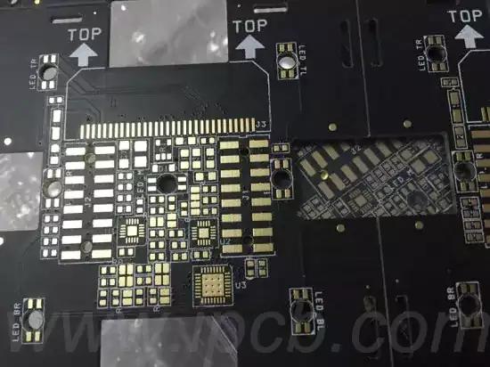
A potting pcb is a circuit board that has been subjected to a special potting process. This process usually involves the potting of a specific part of the board or the entire board surface with a protective insulating material. The potting material not only improves the mechanical strength of the board, but also effectively prevents the intrusion of moisture, dust and other harmful substances, thus enhancing the stability and reliability of the board.
The process of making a potting PCB involves a critical encapsulation step. Through the use of a mold, electronic parts or components are encapsulated and filled with a specific potting material. Once the material has cured, it is removed from the mold to form a robust enclosure. This process not only protects the electronic components inside, but also improves the stability and reliability of the entire board.
When selecting a potting material, a variety of factors need to be considered. First, the thermal properties of the material is an important indicator. Different potting materials have different temperature resistance ranges, so you need to choose the right material according to the operating temperature of the circuit board. In addition, the material’s hardness, elongation, and expansion and contraction characteristics are also key factors to consider. These factors will directly affect the mechanical properties and long-term stability of the circuit board.
The advantages of potted PCB are mainly reflected in the following aspects:
First, excellent waterproof and dustproof performance. The strong shell formed by the potting material can effectively isolate the water and dust in the external environment, protecting the circuit board from erosion and damage.
Secondly, it can withstand harsh environments. Potting PCB is able to directly face harsh operating environments, such as conductive pollutants, chemical erosion, and challenges such as vibration and shock resistance. This makes it promising for a wide range of applications in demanding fields such as automotive electronics and aerospace.
In addition, potting circuit board provide structural reinforcement and electrical insulation. The potting material enhances the mechanical strength of the board and improves its resistance to shock and vibration. At the same time, it can also provide good electrical insulation to ensure the normal operation of the circuit board.
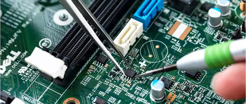
It is worth mentioning that potting circuit board also offer unique advantages in terms of repair and rework. Although the potting material encapsulates the electronic components, the board can be repaired and replaced when necessary by removing the potting material in a specific way. This facilitates the maintenance and upgrading of circuit boards.
However, it should be noted that the manufacturing process of the PCB is relatively complex and requires precise process control and high quality material assurance. At the same time, the selection and use of potting materials need to be based on specific application scenarios and requirements for comprehensive consideration.
With its unique process and significant advantages, potted pcb plays an increasingly important role in the field of electronics. With the continuous progress of technology and application areas continue to broaden, I believe that potting PCB will show a broader application prospects in the future.