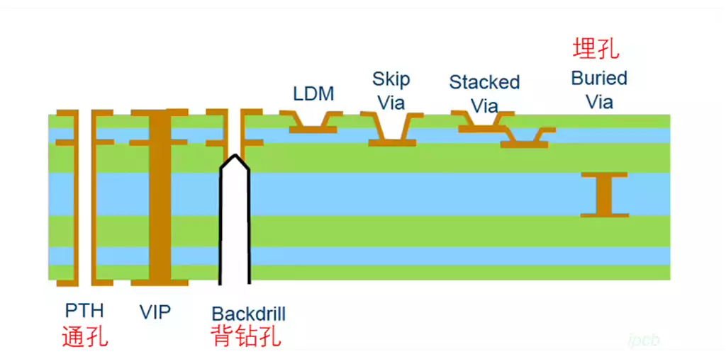
What is via?Through-hole, that is, in the copper cladding board drilling the required holes, it carries on the layer to layer conduction, used for electrical connections and fixed devices. Vias are a vital and indispensable part of PCB production.
On a functional level, perforations are divided into two main categories:
1.For the electrical connection between the layers, to ensure the smooth flow of current between the different layers;
2.They are used to fix or position the devices to ensure the solidity and accuracy of the components on the PCB board.
And from the point of view of the manufacturing process, vias are mainly classified into three types:
Blind vias, which are located on the top or bottom surface of the PCB, and have a certain depth, mainly used to connect the surface layer of the line and the inner layer of the line, its depth is usually limited by the aperture ratio.
Buried vias, which are located entirely in the inner layer of the PCB and do not touch the surface of the circuit board. Both types of vias are located in the inner layer and require a specific through-hole molding process prior to lamination, and may be formed with multiple inner layers stacked on top of each other.
Through-holes, which run the length of the board, can be used either for internal interconnections or as mounting and positioning holes for components. Because the through-hole is easier and less expensive to fabricate in the process, it has become the preferred choice for the vast majority of printed circuit boards in practice, while the other two types of vias are used less frequently. In the following discussion, unless otherwise noted, we will refer to through-holes primarily.
Common vias include vias covered with oil, vias open window, vias plugged with oil, resin plugged and plated to fill holes. Vias are covered with solder resist ink, which is designed to achieve an insulating effect and prevent tin sticking during the later placement and DIP processes. However, special attention needs to be paid to whether via is used for plug-in holes during documentation to avoid soldering problems caused by green oil coverage.
Compared to over-hole cover oil, over-hole windowing leaves the over-hole and hole ring exposed and not covered with soldermask oil. This process increases the heat dissipation area and is suitable for boards with high heat dissipation requirements. It also facilitates measurement work on the vias. However, there is also a risk of shorting out the connecting tin in the vias, so it should be used with caution.
Vias are plugged with solder resist ink during PCB substrate production to prevent short circuits caused by the presence of tin beads inside the vias. If the plugging is not done properly, it may lead to reddening of the hole edges, affecting the appearance and quality.
Resin plugging process is to first copper-plated hole walls, and then use epoxy resin to fill the hole, and again on the surface of the copper plating. This process is commonly used in BGA parts, applicable to the number of layers, board thickness of the product, its surface is flat, the hole can lead and does not affect the welding.
Electroplating hole filling process is through the electroplating of copper to fill the hole, so that the bottom of the hole is flat. This process is not only conducive to the design of stacked holes and holes on the disk, but also improve electrical performance, heat dissipation, improve product reliability.
PCB production in a variety of over via hole process, each with its own characteristics.Correctly select and use the appropriate over-hole process, to ensure the quality and performance of the PCB is of great significance.