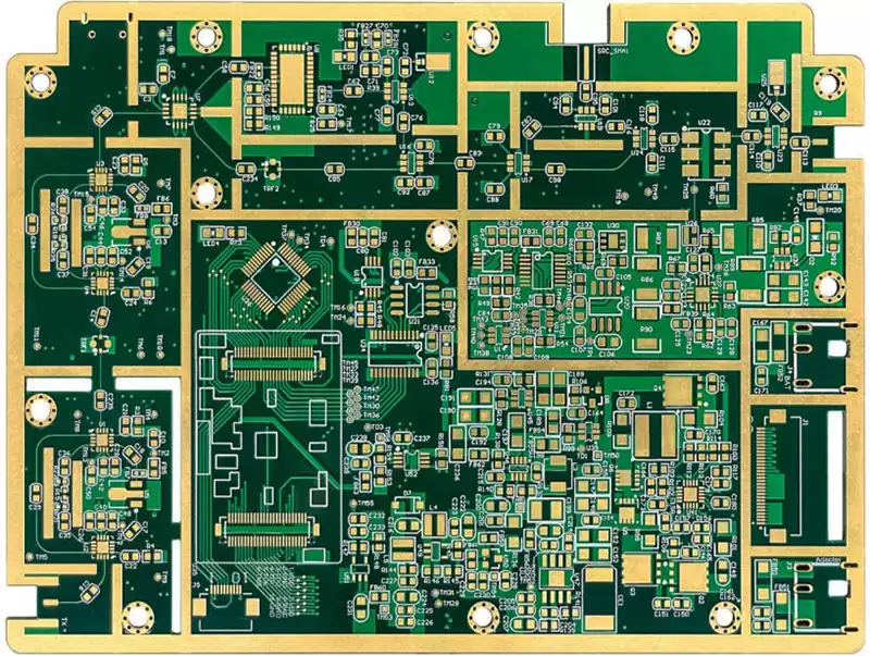
The solder pads, as the basic element of surface mount assembly, forms the core of the circuit board pad pattern, i.e. the combination of pads designed for a specific component type. It is not only a bridge for electrical connections, but also a key part of device fixation, which serves both functions.
In the many types of PCB pads, common square pads, mostly used for larger components and a smaller number of printed wires on a simple printed board, handmade PCB is particularly common. Round pads are widely used in the regular arrangement of components in a single, double-sided printed circuit boards, pads of moderate size to ensure the stability of the welding. Island-shaped pads are characterized by pads and pads between the line into one, suitable for vertical irregular arrangement of the installation scenario. Polygonal pads are used to differentiate pads with similar outside diameters but different hole diameters, facilitating processing and assembly. Oval shaped pads are commonly used for soldering dual in-line devices because of their larger area and increased peel resistance. Open pads are used to ensure that after wave soldering, manual filler pad holes are not sealed by solder.
In terms of special pads, plum pads are used for large over-hole grounding position, which is designed to ensure a good grounding effect, to prevent poor grounding in the installation or disassembly process. Crosshatch pads, also known as hot pads, are designed to reduce heat dissipation during the soldering process and improve the quality of the soldering, and are especially suitable for ground connections and machine patch reflow processes. Teardrop pads, on the other hand, are commonly found in high-frequency circuits and are used to prevent pad skinning and disconnection of the alignment from the pad.

In PCB design, the design of the pad needs to follow a series of standards. First, the shape and size of the pad should be reasonably designed to ensure that the solidity and reliability of the soldering. Calling the PCB standard package library is the key to ensure design compliance. Pad hole size should be moderate, too small is not easy to process, too large may cause unnecessary continuous welding. The spacing between the pads and pads should also be controlled within a reasonable range to ensure soldering quality. In addition, the reliability of the pad design is equally important, including symmetry, pad spacing, the remaining size and width of the reasonable design to ensure that the welded point of solidity and reliability.
As the cornerstone of circuit connection and device fixation, the design of PCB solder pads is of great significance to ensure the stability and reliability of circuit boards. By following the design standards and reliability points, we can ensure that the pads in the soldering process to play the best performance for the normal operation of electronic equipment to provide strong protection.