What is routing in pcb?PCB routing is in accordance with the PCB circuit schematic, wire table and the need for wire width and spacing of printed wires, electronic components can be realized between the line connection and functional realization, but also an important part of the power supply circuit design.
PCB routing has single-sided wiring, double-sided wiring and multilayer wiring. There are two types of wiring: automatic wiring and interactive wiring, before the automatic wiring, can be used to interact with the more stringent requirements of the line in advance for wiring,input and output side lines should be avoided adjacent to the parallel, so as not to produce reflective interference.If necessary,ground isolation should be added, the wiring of the two neighboring layers should be perpendicular to each other, parallel is prone to parasitic coupling.
Automatic wiring of the cloth through the rate, depending on a good layout, wiring rules can be pre-set, including the number of bends, the number of holes, the number of steps, and so on. Generally, the first exploratory cloth warp, quickly connect the short line, and then maze wiring, the first to cloth the connecting line for global wiring path optimization, it can be required to disconnect the cloth has been laid line.And try to re-wire again to improve the overall result.
Order of PCB wiring:
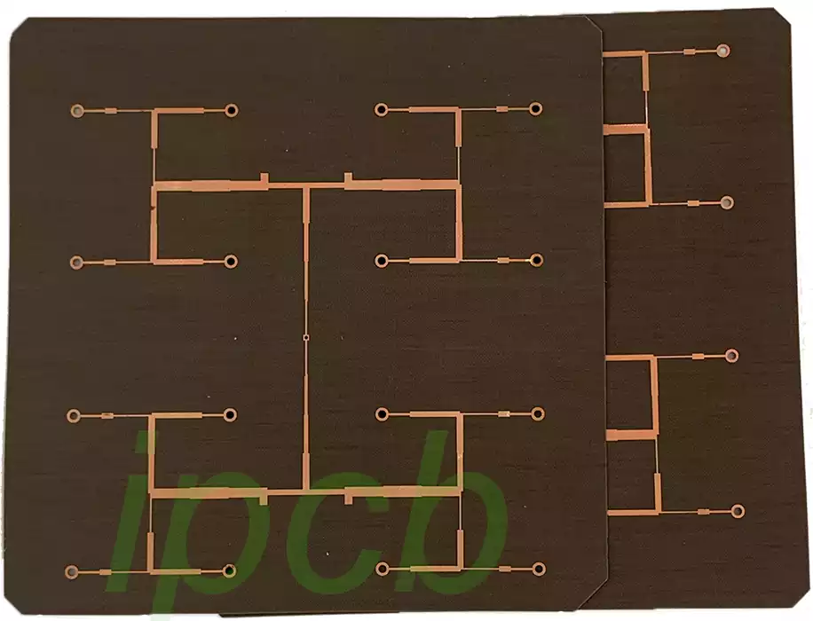
Wiring should be neatly organized, not crisscrossed without rules.These are to ensure that the electrical performance and meet other individual requirements to achieve, otherwise it is the end of the matter, in the design process of printed circuit board,wiring is generally divided into so many three realms:
(1) First of all, the cloth through, which is the most basic requirements of PCB design. If the lines are not cloth through, get everywhere is a flying line, it will be an unqualified board, you can say that not yet started.
(2) followed by electrical performance to meet, which is a measure of a printed circuit board is qualified standard. This is after the cloth through, carefully adjust the wiring so that it can achieve the best electrical performance.
(3) followed by aesthetics, if your wiring through the cloth,there is nothing to affect the electrical performance of the place,but at a glance over the chaotic, plus colorful, flowery,that even if your electrical performance how good, in the eyes of others or a piece of garbage.This brings great inconvenience to the test and maintenance.
Wiring principles
Follow the circuit schematic
Wiring should strictly follow the circuit schematic diagram to ensure that the lines are connected correctly to prevent short-circuit or broken circuit problems. In the wiring process, each component in the circuit should be labeled for subsequent maintenance and repair.
Consider the signal direction
When wiring, you need to consider the direction of the signal, as far as possible to make the signal line the shortest, in order to reduce signal attenuation and noise.For high-frequency signals, attention needs to be paid to the impedance matching of the signal lines to avoid signal reflection and distortion.
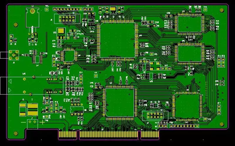
Layered wiring
In a multilayer PCB, the wiring should be layered according to the function of the circuit. For example, the power and ground layers can be routed separately to minimize power and ground noise. Different signal layers can also be wired in layers to avoid interference between signals.
Avoid 90-degree bends
Signal lines should avoid 90-degree bends during transmission. This is because such bends increase signal reflection and noise, affecting the quality of the signal. If a 90-degree bend must be made, a 45-degree bend or a circular bend should be used for the transition.
Ground Design
The design of the ground is critical to the reliability of the PCB. In the wiring process, it should be ensured that the ground line is as wide as possible to reduce the impedance of the ground line and improve the stability of the ground line. At the same time, 90-degree bends in the ground line should be avoided to ensure the continuity of the ground line.
Component wiring rules
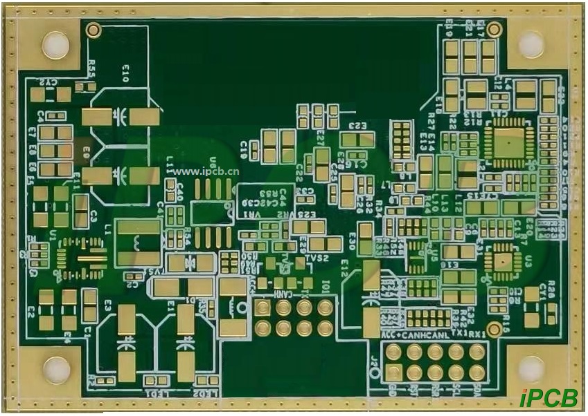
- Drawing wiring area from the PCB board edge ≤ 1mm in the region, as well as the mounting holes around 1mm, prohibit wiring.
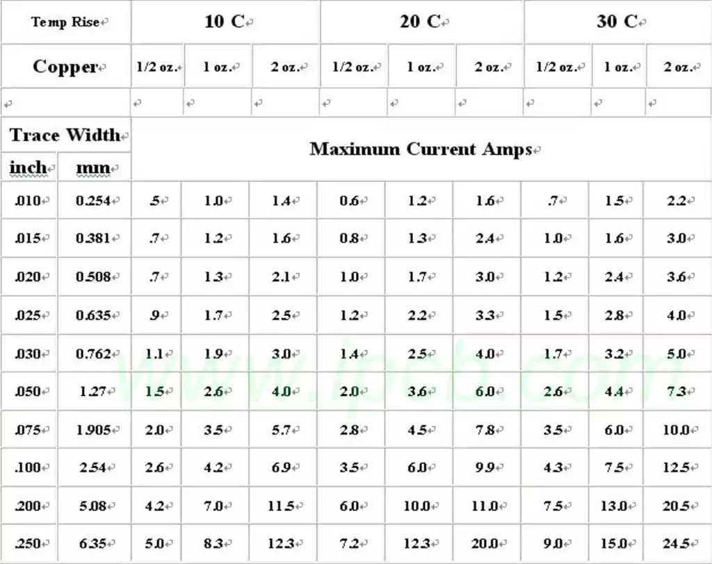
- Power lines as wide as possible, should not be less than 18mil; signal line width should not be less than 12mil; cpu in and out of the line should not be less than 10mil (or 8mil); line spacing is not less than 10mil.
- Normal through-hole should not be less than 30mil.
- Double row direct insertion: pad 60mil, aperture 40mil.
1/4W resistor: 51*55mil (0805 surface mount); pad 62mil, aperture 42mil for direct insertion.
Electrodeless capacitors: 51 * 55mil (0805 surface mount); direct insertion pad 50mil, aperture 28mil. - Note that the power line and ground should be radial as far as possible, as well as the signal line can not appear back to the loop alignment.
PCB routing is an indispensable part of electronic design, it is by virtue of fine line layout and strict specifications to ensure the performance and reliability of the circuit board. By following the wiring principles, we can achieve the optimized design and excellent performance of electronic products.