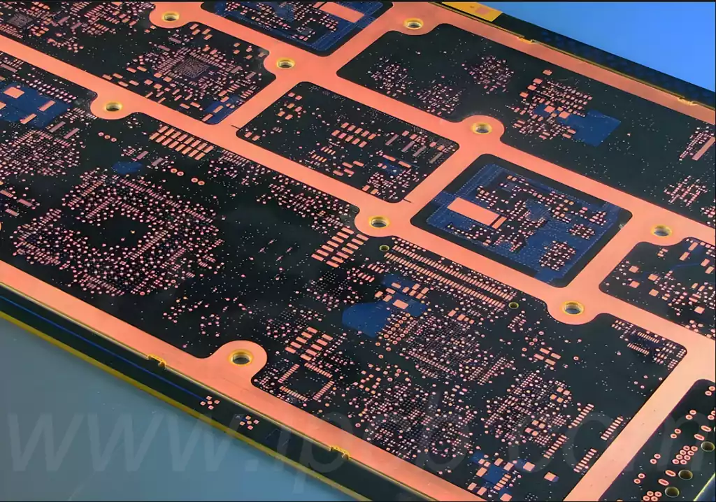
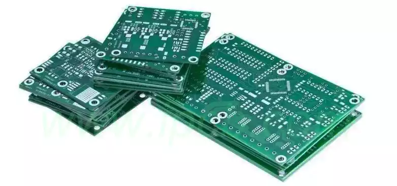
PCB Via fill is a material used to fill through holes in a PCB board. Through holes are holes punched in a PCB to connect different circuit layers so that current or signals can flow through. The purpose of through-hole fillers is to prevent liquid solder pads or other impurities from remaining in the through-holes, while improving the mechanical strength and durability of the PCB board.
PCB via filling can be categorized into organic through-hole fillers and inorganic through-hole fillers. The main pcb components of organic through-hole filler are epoxy resin and hardener, with better adhesion and heat resistance; inorganic through-hole filler is mainly composed of glass fiber, alumina, silicon oxide and other pure inorganic substances, with better mechanical strength and durability. According to different application scenarios and requirements, different types of through-hole fillers can be selected.
Sometimes it is necessary to fill PCB through-holes, for example to reduce the risk of trapping air or to increase conductivity. Some common methods of filling through-holes include.
- Through Tenting
Through-hole tenting creates a soldermask layer over the PCB via instead of filling the hole with material.This can be a quick,easy and cost-effective option for covering through holes, but tented vias may re-open over time.
Tented Through-Hole Applications
Protect solder float to component side
Enabling vacuum adaptation in production
Cover critical via holes, such as under BGA
- Via Plugging
The through-hole plugging process fills the hole with non-conductive material and seals it with a mask. Through-hole plugging also covers the annulus and does not produce a smooth, glossy surface.
Application
Protecting the solder float to the component side
Enabling vacuum adaptation in production
- Via Filling
Through-hole filling uses resin to create a permanently filled hole. Through-hole filling is a common type of through-hole filling in which the manufacturer fills the through-hole with a conductive material, plates the surface with copper, and then trims the surface. This process allows signals to be routed to other areas of the PCB.
Applications
Space saving
Protects solder floating to the component side
Facilitates stacking and interleaving of microvias for sequential build-up of multilayers (SBU)
Facilitates in-pad through-hole technology, such as BGAs
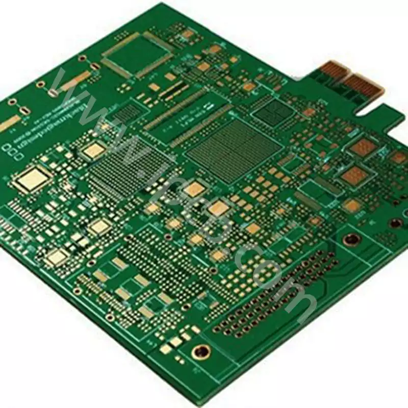
Through-hole fillers are widely used in electronics manufacturing. In cell phones, for example, there are many small PCBs inside the phone that require through-hole fillers to improve mechanical strength and prevent residue, as well as to prevent incorrect connections between electronic components. Through-hole filler is not only widely used in cell phones, but also has important applications in other electronic products, such as tablet PCs, smart watches, laptops and so on.
Wave soldering through-hole filling poor factor analysis
- The weldability of the material (component pins and PCB through holes and pads) determines the wettability of the interface, affecting the height of the through-hole filling.
- Flux selection and coating.
Selection: determines the solderable end of the oxide film film removal process capabilities, affecting the solderable end of the solder wetting properties of the solder face.
Coating: Coating uniformly in place, so that all the inside of the hole wall is uniformly coated, so that the solder can climb into place.
- Equipment maintenance: pay special attention to the preheating performance of the equipment, must ensure that the board preheating uniformity and the temperature of the back of the board to reach the target value, otherwise affect the solder climb.
- Wave soldering parameters set: track inclination, chain speed, flux spray volume, flux spray uniformity, preheating temperature and time, welding temperature and time, the height of the wave and other process parameters
- Matching of PCB aperture and component pin diameter.
- Through-hole blocking installation (pins at the bottom of the component body, installed close to the board, hindering the flow of molten solder, resulting in the inability to exhaust, resulting in insufficient fill rate)
Component pins ≥ 3.5g each, components can take the standoff mounting (limit pads)
Components between the bottom surface and the PCB raised 0.3-2.0mm, the specific requirements to consult the IPC-A-610H-7.1.6 or QJ3012-5.7.2, the gap should be controlled at a minimum, in order to be used to ensure that the bending distance due to vibration and shock caused by the smallest possible.
7.PCB through-hole pads exist in the ground layer, heat dissipation layer, did not do thermal pad processing
Design standard: GJB4057A-2021 QJ3103A-2011
Thermal pad width = through-hole pad diameter × 60% ÷ number of channels
PCB Via fill is a key link in PCB manufacturing, which is vital for enhancing the performance and reliability of electronic products. With the advancement of technology, its application will be more extensive, promoting the development of electronic products to a higher standard.