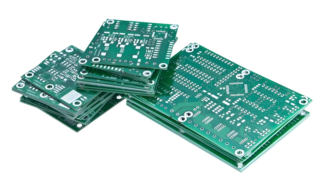
VIPPO (Via in Pad Plated over) is an over-hole technology, mainly used in PCB boards.POFV is Plating Over Filled Via abbreviation, refers to the PCB on the over-electrical holes, in order to meet the needs of the soldering and over-hole internal conduction, the first over-hole resin plugging holes, and then copper-plated to cover the holes on the resin layer of the practice, referred to as the POFV process. POFV process, also called VIPPO.
The POFV process can be divided into two parts: the first half is called “drilling” and the second half is called “plugging”.
The holes are processed in a variety of ways, including through holes, blind holes, countersunk holes, back drilling, etc. Among these, through holes are generally used for plating. Among them, through holes are generally used for copper plating, and the process of plugging holes includes full plugging, half plugging, VIPPO and SKIPPO.
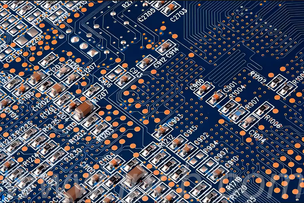
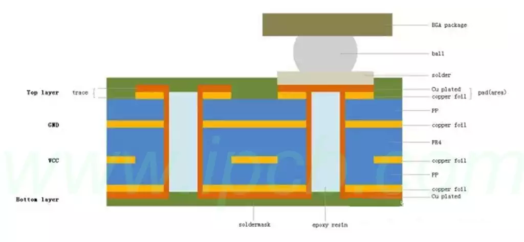
If you need to drill holes in pads and paste electronic components, you must use VIPPO (Via in Pad Plated over) or SKIPPO (Skip Via in Pad Plated over).VIPPO and SKIPPO are generally used on BGA pads.
Among them, VIPPO over holes can be through holes or blind holes; while SKIPPO over holes specifically refer to blind holes from the top layer to the third layer, and from the bottom layer (n) to the n-2 layer.
The diameter of VIPPO should not exceed 0.5mm, otherwise solder paste during SMT may flow into the hole, or flux may flow into the hole during heating, which may generate gas and lead to insufficient connection strength. Between the device and the pads, there will be virtual soldering.
The cost of PCB board will increase by 15%~25% after using VIPPO process. The pads are easy to come off during soldering, try to choose packages with large pin spacing. In that case, why do we need to use VIPPO?
Because VIPPO greatly improves the PCB board wiring density, especially in the BGA area. Some information also gives the role of eliminating capacitive effects, normal BO / BO below a ground layer, resulting in capacitive effects, VIPPO eliminates capacitive effects.
Advantages of pofv process:
The hole-in-disk process makes the process three-dimensional, effectively saves space and adapts to the development needs. In general, the use of vacuum hole plugging machine, so that the quality of hole plugging is more stable.
The use of POFV process, can improve the efficiency of PCB design engineers, and PCB yield, because in the design of the over-hole will take up too much space resulting in difficult wiring, the designer shall use a thin line such as 3.5 mil line width or smaller.And over-hole in the pad, giving up a lot of space, the designer can use more space for wiring;
For high-speed and high-frequency boards, this is good for performance and better for electrical performance.
Process flow:
1.Open material drilling
According to the requirements of the engineering data MI,in line with the requirements of the large sheet,cut into small pieces of production boards,small pieces of sheet material in line with customer requirements,according to the engineering data,in the opened in line with the requirements of the size of the sheet material, the corresponding position of the requested aperture drilling.
2.Copper sinking
Copper deposition is the use of chemical methods to deposit a thin layer of copper on the wall of the insulation holes.
3.Graphic transfer, electroplating, decoating
Graphics transfer is the production of film on the image transferred to the circuit board, in the line graphic exposed copper skin or hole wall plating a layer of copper to achieve the required thickness and the required thickness of the copper layer and the required thickness of gold and nickel or tin layer. With Na0H solution to retire the anti-plating cover film layer so that the non-line copper layer is exposed.
4.Green oil, tin plate, test
Process flow chart:
Pre-processing → drilling through the hole (only drilling out the holes need to be resin plug holes) → immersed copper 1 → plating 1 → QC inspection → resin plug holes → baking board → grinding the hole resin → drilling other holes → immersed copper 2 → plating 2 → post-processing.
To make a POFV PCB,the face copper needs to be plated twice, once when the hole in the disk is plated with hole copper, once when the non-disk hole is plated, and once when the other non-disk hole is plated.In accordance with the provisions of IPC-A-6012 inside,the smallest over-hole copper level II is 18um, the average hole copper is 20um, level III is the smallest 20um, the average hole copper is 25um. if in accordance with the IPC level II standards, the use of 1/3 OZ base copper production, the final thickness of the PCB surface copper in the done POFV, probably 12um (base copper) + 20um (hole copper in the disk) +20um (non-disk hole hole copper), the total copper thickness of about 52um.
If the POFV design of the PCB, the outer layer of the line width line spacing is less than 3.5/3.5mil, due to plating the printed circuit board outer layer of copper is too thick, resulting in etching the line thin or open circuit.
Current PCB design, the outer layer of the line width spacing is only 3/3.34mil, if the resin plug holes, the production process will be difficult to control the quality.
0.5mmBGA, the disk elsewhere in the disk hole design, line width line spacing optimization is less than 3.5mil.
Optimized effect, the outer layer of the line to move to the inner layer to go,BGA PAD to play the hole in the plate, because the other places in the plate also have a hole in the plate, do not care more about the few holes in the plate,the production yield rose a lot, the cost is reduced.
POFV process with its unique advantages in PCB design to show its important role in improving wiring efficiency and safeguard electrical performance. Through optimized design and fine process control, we are not only able to overcome technical challenges, but also improve production yields and reduce costs. Looking ahead, the VIPPO process will continue to bring more innovations and breakthroughs to the PCB design field.