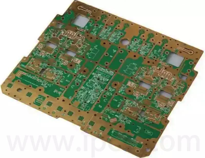
A double sided PCB board (or 2-layer PCB) is a printed circuit board coated with copper on both sides, top and bottom. There is an insulating layer in the middle. To use circuits on both sides, there must be a proper circuit connection between the two sides. The ‘bridge’ between such circuits is called a via. Vias are small holes in the PCB that are coated with metal and can be connected to the circuits on both sides.
Double sided pcb board is typically used in applications that require higher circuit density and more complex circuit designs. Compared to single-sided PCBs, double sided PCB board can accommodate more circuit components in the same board size, thus allowing for more complex circuit designs. Dual-sided PCBs typically use two-sided wiring, which allows circuits to be connected on both sides by threading them through holes between the two sides. This approach greatly increases the density and reliability of the board.
Features and benefits of double sided PCB boards:
1.2 layer PCB can be laid on both sides of the components and circuit connection lines. Compared with the single sided PCB board, its available space is larger, so it is suitable for some electronic products that require dense wiring, many devices, complex circuit connections between components.
- Because there are two sides available, so the double sided PCB board can reduce the wiring area, so as to achieve a comprehensive reduction in the area of the PCB board for the purpose of saving costs and space.
- The path of 2 layer PCB board is generally shorter than single-sided PCB boards, thus reducing the overall resistance and power loss of electronic devices.
- Because 2 layer PCBs have more complex connections, they are able to support more devices, allowing designers to be more flexible in designing circuit boards for more functionality and performance.
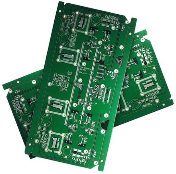
On the other hand, double sided PCB boards have their drawbacks:
- The manufacturing cost of 2 layer PCB is relatively high because the process is more complex than that of single sided PCB boards,which requires longer manufacturing time and more manpower and material costs.
- 2 layer pcb requires more devices,so their design and wiring are more complex and require a higher level of skill and experience.
When designing 2 layer PCBs, choosing the right materials is a key factor in ensuring the performance and reliability of the boards:
1.Substrate Material
FR-4.
A widely used glass fibre reinforced epoxy resin material with good mechanical and electrical properties for most applications.
HF Materials.
Materials such as Rogers, suitable for high frequency and high speed applications, offering excellent electrical properties.
Polyimide (PI).
Used in flexible circuit boards, with good resistance to high temperatures and flexibility, suitable for applications where space is limited or bending is required.
- Conductive Layer Materials
Copper Foil.
The conductive material used in most double sided pcb boards. The thickness of the copper varies depending on the needs of the application, and is usually 1/2 ounce to 1 ounce, or even thicker (e.g., in high-power applications).
- Surface Finishing Materials
HASL (Hot Air Levelling).
A traditional surface finish that provides good solderability, but may not be suitable for fine pitch soldering.
ENIG (Electroless Nickel and Gold Plating).
Provides better solderability and corrosion resistance, and is suitable for high-end electronic devices that require higher surface finishes.
OSP (Organic Sealer Sheet).
Environmentally friendly surface treatment material, can keep the system clean after use, suitable for short time assembly and welding.
4.Insulation Material
Solder Resist Ink :Solder Resist Ink.
Used to cover unconnected wires to prevent short-circuiting while providing some mechanical protection, common colours include green, blue and black.
5.Other Special Materials
Thermal Conductive Materials.
Used in high power or heat sensitive applications, this material maintains the normal operating temperature of the circuit by increasing the thermal conductivity.
Antioxidant Coatings: These are used in applications where high humidity or corrosive environments are present.
Used in high humidity or corrosive environments to protect the board surface and copper layer from oxidation.
Double sided PCB boards occupy an important place in modern electronic equipment due to their high density, reliability and design flexibility. Correct material selection and careful design is the key to ensure its performance and reliability, providing a solid foundation for electronic equipment innovation.
