With the rapid development of modern communication technology, high frequency PCB communication circuits have gradually become the core component of various electronic devices. In order to ensure the stable performance and signal quality of high frequency communication circuits in high frequency environments, the optimisation of signal integrity (SI) is particularly important.
1.Separation
Components on a PCB circuit have different edge rates and noise variances. In order to most directly improve signal integrity (SI), this can be achieved by physically separating the components on the PCB circuit according to their edge rates and sensitivities. Figure 1 provides a concrete example. In this example, circuits with high risk to clock and data conversion circuits, such as power supplies, digital input/output ports, and high speed logic circuits, require special attention and separation.
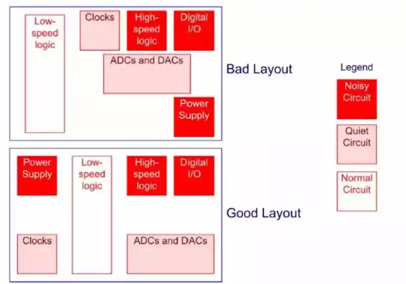
In the first layout, the clock and data converters are placed close to the noise source devices, which can lead to noise coupling into the sensitive circuits, thereby degrading their performance. In contrast, the second layout significantly improves the signal integrity of the system design by implementing effective circuit isolation.
2.Impedance control, reflection and termination matching strategies
Impedance control and termination matching play an important role in high frequency communication circuits design. Although RF circuits are regarded as a core part of most circuit designs, some digital circuit designs, whose frequency is even higher than that of RF, often neglect the importance of impedance and termination matching.
Impedance mismatch can cause a number of problems that pose a serious threat to digital circuits, as follows:
a.Between the input of the receiving device and the output of the transmitting device, digital signals are reflected. These reflected signals propagate back and forth along the transmission line until they are eventually completely absorbed.
b.Reflected signals cause an oscillating effect (i.e., ringing effect) of the signal on the transmission line, which in turn affects the voltage stability, signal delay, and may result in a serious degradation of the signal quality.
c.An impedance mismatch signal path may also cause the signal to radiate into the surrounding environment, resulting in unwanted interference.
To mitigate the problems caused by impedance mismatch, reflections can be minimised by adding terminating resistors to the signal line near the receiving end. This terminating resistor usually consists of one or two discrete devices and is simply a small resistor in series. The purpose of the terminating resistor is to limit the rise time of the signal and to absorb some of the reflected energy. It is worth noting, however, that while impedance matching can mitigate destructive effects, it does not eliminate them completely. Therefore, careful consideration should be given when selecting a suitable device to ensure that the termination impedance is effective in controlling signal integrity.
Not all signal lines require impedance control.For some specific specification requirements, such as compact PCI, characteristic impedance and terminating impedance characteristics are necessary.However,the situation is different for other standards that do not specify impedance control requirements, or for scenarios where the designer has not given special attention.The final standard may vary from application to application. Therefore, the length of the signal line (related to the delay Td) as well as the rise time of the signal (Tr) need to be taken into account when deciding whether or not to perform impedance control. In general, impedance control should be considered when the delay Td is greater than 1/6 of the rise time Tr.
3.Internal Power Layers and Their Segmentation
One aspect of current loop design that is often overlooked by designers in digital circuit design is the consideration of single-ended signals travelling between two logic gates (refer to Figure 2). Specifically, current flows from logic gate A to logic gate B and subsequently returns to logic gate A through the ground plane, forming a complete current loop.
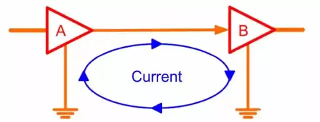
There are two major potential pitfalls in the gate current loop:
a. The ground plane between points A and B needs to be connected via a low impedance path.
If the connection impedance between the ground planes is high, a voltage back-up will occur between the ground plane pins. This will inevitably lead to signal amplitude distortion in all devices and increase the superposition of input noise.
b. The area of the current return loop should be as small as possible
The loop is like an antenna. Typically, the larger the loop area, the greater the chance of radiation and conduction. Every circuit designer expects the return current to flow directly along the signal line, thus creating the smallest loop area. Large area grounding solves both of these problems. Not only does large-area grounding provide a low-impedance connection to all grounding points, but it also allows the return current to follow the signal line as directly as possible.
A common mistake in PCB design is to randomly punch holes and slots between layers. Figure 3 shows the direction of current flow when a signal line traverses an area with slots cut in different layers. At this point, the loop current will have to bypass the slots, thus creating a larger loop current loop.
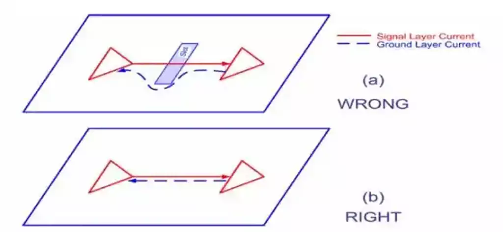
Generally, slots should not be cut in the ground power plane. However, in some cases where a slot has to be created, the PCB designer must first make sure that there are no signal loops passing through the slotted area.This principle also applies to PCB design for mixed-signal circuits, unless multiple ground planes are used. Especially in high-performance ADC circuits, mutual interference between signals can be effectively reduced by separating the ground layers of analogue signals, digital signals and clock circuits. It is important to note again that where slotting is necessary, the designer must first and foremost ensure that there are no signal loops traversing the slotted area.
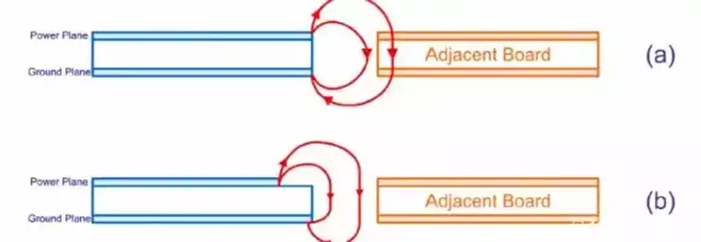
In addition,in the design of power supply layers with mirrored differences,attention also needs to be paid to the area of the interlayer area (as shown in Figure 4). The power plane layer at the edge of the board may have a radiation effect to the ground plane layer, and electromagnetic energy leaking from the edge may interfere with neighbouring boards (see Figure 4a). To mitigate this effect, the area of the power plane layer can be appropriately reduced (see Figure 4b) so that the ground plane layer overlaps it in a specific area. This reduces the electromagnetic leakage and thus the interference with neighbouring boards.
- Crosstalk phenomenon
In PCB design, crosstalk is an important issue that should not be ignored. The figure below shows the crosstalk area between three pairs of adjacent side-by-side signal lines on a PCB circuit and their associated electromagnetic fields. When the spacing between the signal lines is too small, the electromagnetic field between them will interfere with each other, resulting in signal changes, this phenomenon is crosstalk.
An effective way to solve the crosstalk problem is to increase the spacing between signal lines. However, with the increasing tightening of wiring space and shrinking of signal line spacing, PCB designers are often faced with the challenge of introducing crosstalk into their designs. Therefore, PCB designers need to have some ability to manage crosstalk problems. The 3W rule, commonly followed in the industry, recommends that the spacing between adjacent signal lines should be at least three times the width of the signal line. However, in actual engineering applications, the acceptable signal line spacing depends on specific application scenarios, operating environment and design redundancy and other factors. The determination of signal line spacing needs to be calculated and adjusted according to the specific situation.
When crosstalk problems cannot be avoided, a quantitative assessment of crosstalk is required. This can be achieved through computer simulation techniques. Using a simulator, the designer can assess signal integrity and the impact of crosstalk on the system to make more informed design decisions.
- Power decoupling technology
Power supply decoupling is a routine practice in digital circuit design that helps reduce noise problems on the power line. High frequency noise superimposed on the power supply may cause interference to adjacent digital devices. These noises usually originate from ground bounce, signal radiation, or the digital devices themselves.
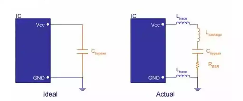
The easiest way to solve the power supply noise problem is to decouple the high frequency noise using capacitors. The ideal decoupling capacitor provides a low impedance path to ground for high frequency noise, thus eliminating power supply noise. When choosing a decoupling capacitor, the designer needs to make a choice based on the actual application. Most designers will choose to install surface mount capacitors near the power supply pins and ensure that their capacitance is large enough to provide a low impedance path to ground for predictable power supply noise.
However, there are some issues to be aware of when using decoupling capacitors. The package of the capacitor may introduce parasitic inductance, and the capacitor itself may introduce some equivalent resistance. In addition, the wires between the power pins and the decoupling capacitor and the wires between the ground pins and the ground plane can also introduce equivalent inductance. These factors may result in the following effects:
a. Capacitance may induce a resonance effect at certain specific frequencies, which can increase the network impedance and have a greater impact on signals in adjacent frequency bands.
b. Equivalent resistance (ESR) may also affect the decoupling effect on high-speed noise, thus affecting the formation of low-impedance paths.
Optimising the signal integrity of high frequency PCB communication circuits is a critical task that requires the designer to consider multiple aspects, from physical separation to impedance control, to power management and crosstalk suppression, with each step carefully planned. As technology continues to advance, these design challenges will become more complex, but also offer endless possibilities for innovation.
