Why do we need to test circuit boards?
- Maintaining good quality:
Although PCBs are produced correctly in most cases, no one can ensure that there will be no errors in PCB production. Therefore, the work of testing circuit boards is carried out during or after the completion of the PCB. PCB manufacturers detect circuit boards with open circuits or short circuits. - Complying with industrial standards:
Almost all industrial fields have their acceptance standards. In the PCB production industry, the most widely accepted standards are IPC standards, such as IPC-A-600. PCB manufacturers will perform many tests to ensure that the PCBs are produced and meet the standards, such as copper thickness, plating thickness, defects, etc. - Meeting customer needs:
In addition to following industrial standards such as IPC, PCB production has its own requirements. For example, PCBs with impedance traces need to do TDR testing to ensure that the impedance value meets customer requirements. - Troubleshooting and error detection:
One of the main advantages of PCB testing is that it helps to find errors in the final PCB, whether the error is related to mechanical or electrical functions, which ultimately helps to troubleshoot PCB failures. - Cost Saving:
Although additional test circuit board requires more time and investment in production, and any serious defects can cause great losses to the PCB manufacturer and the customer. So compared to this loss, PCB testing can save a lot of money. - Improved Safety:
Since PCBs have become a necessity in all electronic devices ranging from daily use devices to health and safety devices, the failure of such devices may lead to serious consequences due to PCB failure. For example, a short-circuited PCB may cause a fire or a very serious accident. Testing in the early stages of manufacturing such devices reduces PCB failures and ultimately reduces the potential damage caused by faulty devices, thereby improving safety.
how to test a printed circuit board
Testing circuit board methods, how to test PCBs? Generally speaking, PCB manufacturers provide different PCB testing methods to customers when placing PCBs, and some of them are highlighted below:
Visual inspection:
This inspection is done manually by a trained operator with the help of a microscope or a simple magnifying glass and is considered to be one of the most widely used testing methods. There are many reasons why this testing method is considered to be a widely used method, such as low operating costs and the test procedures can be flexibly changed according to the PCB.
In-circuit test (ICT):
ICT, or automatic in-circuit test, is a must-have test equipment for modern PCB manufacturers and is very powerful. It mainly detects open circuits, short circuits, and faults of all parts of the PCBA by contacting the test points on the PCB layout with test probes, and clearly informs the staff.
ICT has a wide range of uses, high measurement accuracy, and clear indication of detected problems. Even workers with average electronic technical skills can easily handle problematic PCBAs. The use of ICT can greatly improve production efficiency and reduce production costs. It covers a wide range of fault detection and verification of electronic circuits and electronic components, such as short circuits, open circuits, and incorrect component placement. This test can be performed with the help of a bed of nails to check different electronic parameters in newly manufactured PCBs, such as inductance, resistance, and capacitance.
Flying probe test:
Flying probe testing is considered cheaper than ICT. Both can effectively find production quality problems, but flying probe testing has proven to be a particularly cost-effective way to improve circuit board standards and is usually performed without powering the PCB. This test helps to check for open or short circuits, capacitance, inductance, and resistance. This is performed with the help of a probe with a needle. This test is slower and more error-prone than ICT, but cheaper, so for large-volume orders, ICT is more cost-effective.
X-ray inspection:
X-ray inspection is X-ray testing, which uses low-energy X-rays to quickly detect problems such as open circuits, short circuits, empty solder joints, and leaky solder joints on the circuit board.
X-ray is mainly used to detect defective circuit boards with ultra-fine pitch and ultra-high density, as well as defects such as bridging, chip missing, and misalignment generated during the assembly process. It can also use tomography to detect internal defects in IC chips. This is the only way to test the quality of ball grid arrays and solder ball bonding. The main advantage is that BGA solder quality and embedded components can be checked without spending on fixtures.
X-ray testing is performed to check PCB defects that cannot be seen by the naked eye, such as PCB inner layer defects, solder voids, solder joints under BGA or other IC packages, insufficient solder, component misalignment, and inner layer misalignment. X-ray testing is beneficial for complex multi-layer densely packaged PCBs.
Functional testing:
In order to check whether the manufactured PCB performs the intended function correctly, functional testing plays an important role. This test varies from PCB to PCB. A predefined test procedure with relevant equipment is required to perform functional testing by simulating real-world operating conditions.
Environmental Testing:
This test procedure is designed to check the reliability of the manufactured PCB by subjecting the PCB to extreme environmental conditions such as high temperature, low temperature, humidity, shock, vibration, and even extreme temperatures in operation. This reliability test can evaluate the durability and long-term performance of the PCB.
Another thing that needs to be introduced is the functional circuit test.
Functional circuit testing (FCT) is a test that basically checks the functional and electrical performance of the entire circuit. The test ensures that all components in the board work together and no errors occur during operation. During this test, the manufacturer also ensures that there are no shorts or opens in the traces and then provides a pass or fail decision on the finished PCB. Therefore, FCT is one of the important tests performed to ensure that the board is achieving optimal function as expected.
Advantages of FCT? FCT is a powerful and effective method for analyzing performance and gaining important insights into the behavior of the board. The test procedure also allows problems to be identified before the actual manufacturing of the prototype, thereby reducing manufacturing costs. Other benefits associated with functional circuit testing include:Some PCBs may not meet their specified performance requirements due to physical defects on the PCB, such as cracks, pinholes, missing components, missing solder mask, etc. FCT helps detect such errors. The test helps verify that each component on the board can actually perform its function and there are no problems such as crosstalk, impedance issues, or excessive power consumption analysis.
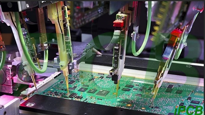
Circuit testing must also be able to check whether the components have been properly soldered. Therefore, this test ensures that the PCB operates as designed and will not cause any problems later. Overall, FCT prevents the development of costly defective products during the production process. The test provides the most comprehensive view of signal behavior such as signal distortion, incorrect voltage/current and power integrity, as well as discovering incorrect component values and field parameter failures. Through a combination of connecting cables, test probes, and test software, the technology can also trigger detailed root cause analysis.
It goes without saying that if you want your PCB to operate effectively, then you should test circuit board properly. Functional circuit testing is very useful in identifying functional and safety-related failures such as stuck, open, short, etc. Therefore, it is always recommended to contact the manufacturer, which means that special emphasis is placed on testing the PCB at every stage of design and production. Almost all well-known PCB manufacturers have powerful test tools, probes and software to check the overall function of the PCB.
So, what are the test points on the circuit board?
How many people know about test points but don’t understand their purpose?
Basically, the purpose of setting test points is to test whether the components on the circuit board meet the specifications and solderability. For example, if you want to check whether there is a problem with the resistor on a circuit board, the easiest way is to use a multimeter to measure its two ends.
Smart engineers invented test points, which lead to a pair of small circular dots at both ends of the parts. There is no solder mask on them, so that the test probes can contact these small dots without directly contacting the electronic parts being measured.
In the early days, when circuit boards were still traditional plug-ins, the solder pins of parts were indeed used as test points, because the solder pins of traditional parts were strong enough and not afraid of needle piercing, but there were often misjudgments of poor probe contact. Because after general electronic parts are tinned by wave soldering or SMT, a residual film of solder paste flux is usually formed on the surface of the solder. The impedance of this film is very high, which often causes poor contact of the probe.
Therefore, at that time, it was often seen that the test operators on the production line were holding air spray guns and blowing desperately at the board, or wiping the places that needed to be tested with alcohol. In fact, the test points after wave soldering will also have the problem of poor contact of the probe. Later, after the prevalence of SMT, the situation of test misjudgment was greatly improved, and the application of test points was also greatly given an important task.
Because SMT parts are usually very fragile and cannot withstand the direct contact pressure of the test probe, the use of test points can avoid the probe directly contacting the parts and their solder pins, which not only protects the parts from damage, but also indirectly greatly improves the reliability of the test, because the misjudgment situation has become less.
However, with the evolution of technology, the size of circuit boards is getting smaller and smaller. It is already a bit difficult to squeeze so many electronic parts on a small circuit board, so the problem of test points occupying circuit board space is often a tug-of-war between the design end and the manufacturing end.
The appearance of the test point is usually round, because the probe is also round, which is easier to produce and it is easier to bring adjacent probes closer together, so as to increase the density of needle bed implantation.
If the adjacent holes are too small, in addition to the problem of contact short circuit between the needles, the interference of the flat cable is also a big problem. It is impossible to implant needles next to some high parts. If the probe is too close to the high parts, there is a risk of collision with the high parts and damage. In addition, because the parts are high, it is usually necessary to open holes on the needle bed of the test fixture to avoid them, which indirectly causes the inability to implant needles. It is becoming increasingly difficult to accommodate the test points of all parts on the circuit board.
Testing circuit boards is very important in the electronics manufacturing industry to ensure that the manufactured PCBs meet the highest standards of functionality, reliability, durability and quality. Whether you are a PCB engineer or a buyer, it is important to understand test circuit boards and how to test PCBs.
