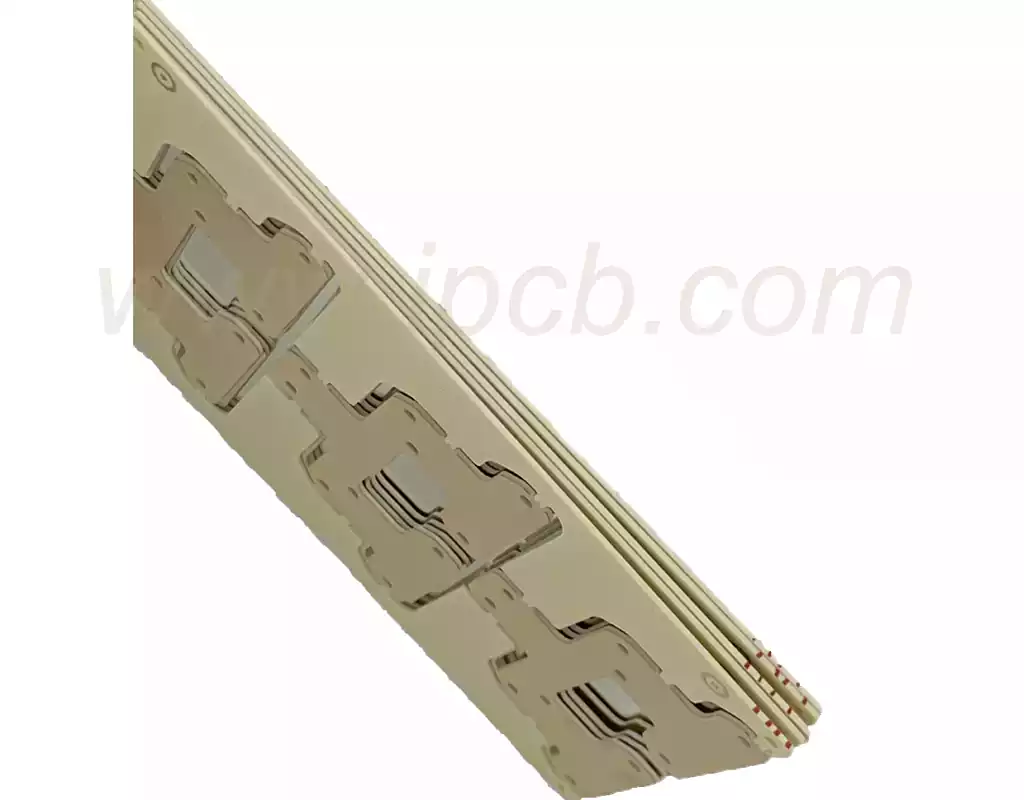
A countersunk hole is a semi-penetrating hole in a circuit board made with a flat head drill or gong cutter, characterised by the fact that the hole does not run through the entire circuit board. Between the outer edge of the hole (i.e., the location of the largest hole diameter) and the wall of the hole at the small aperture, there exists a parallel to the PCB board surface of the articulation part, the articulation part of a flat surface, not bevelled, which is responsible for connecting the large hole area and the small hole area.
Classification of Countersunk Hole
Single round corner countersunk hole
Single round countersunk hole combines the design features of a flat-bottomed hole with a chamfered corner to prevent damage to the head of the screw due to overstretching.These countersunk holes are typically used where screws need to be fastened to sheet metal.
Double Round Countersunk Hole
Double rounded countersunk hole is characterised by the chamfering of both corners. The chamfering of the hole wall increases the contact area between the head of the screw and the hole, which in turn increases the tightening torque and overall durability. This type of countersunk hole is often used when screws or bolts need to be mounted on thin steel plates.
Cylindrical countersunk head hole
Cylindrical countersunk hole presents a rounded countersunk hole pattern, and are particularly suitable for connecting plates with large thicknesses. Its structure is characterised by a protruding bottom surface,a larger hole diameter in the lower part and a smaller hole diameter in the upper part, and an inclined design on both sides of the inner wall of the hole.
Conical Countersunk Hole
Conical countersunk hole presents a tapered hole pattern with chamfers on the wall to carry high strength and high profile joining materials such as injection rivets, plastic washers or bellows.
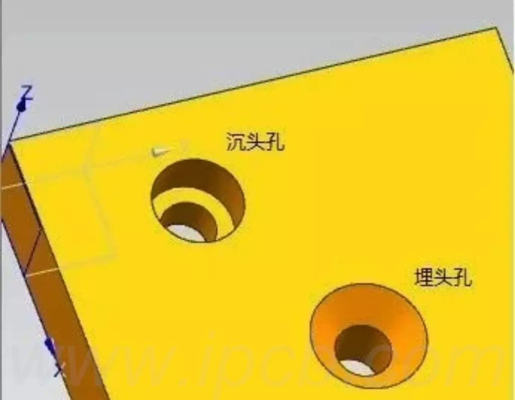
The manufacture of countersunk hole involves a series of complex processes, including the following key steps:
Drilling process:Firstly,a drilling operation is carried out on the PCB using a specialised drill bit precisely tailored to the specific design requirements.The holes created in this step are straight and have the same top and bottom aperture.
Chemical copper deposition step:Next,the surface of the hole wall is uniformly covered with a thin layer of copper by electroplating or chemical deposition. The purpose of this step is to prepare the surface for the subsequent plating and filling process.
Chamfering of the orifice: Subsequently, the orifice is machined by mechanical or chemical means to form an inward sloping surface, thus giving the shape of a countersunk head. During this step, the accuracy of the angle and depth needs to be strictly controlled to ensure the flatness of the orifice and compliance with the design requirements.
Plating and filling process: On the basis that the hole has assumed the shape of a countersunk head, a plating operation is carried out to fill it with copper or other metallic materials. The purpose of this step is to make the aperture a connection channel with good electrical conductivity.
Surface treatment: Finally, the soldermask coating, screen printing of characters and other conventional surface treatment steps, thus completing the entire production process of countersunk head holes.
The application of countersunk hole in PCB circuit boards is very common, especially for the following situations:
Effective use of space:countersunk hole is designed so that they appear only on one side of the board, not through the entire board thickness, thus achieving effective space saving on a limited board area, which is particularly suitable for high-density packaging and miniaturisation of electronic equipment needs.
Appearance beautification:The structure of countersunk hole makes the component mounting surface smoother, without protruding holes, which not only improves the overall visual effect of the product,but also helps to reduce the adhesion of dust, which in turn improves the reliability of the product.
Improved soldering performance:For components that need to be soldered in place through holes (e.g., certain connectors, sockets, etc.), countersunk holes provide a larger contact area,which enhances the strength and stability of the soldering.
Meet special application scenarios:In special application scenarios such as high-frequency circuits and RF modules,countersunk holes can effectively reduce signal interference and improve the overall performance of the circuit.
With their unique design and fine manufacturing process, countersunk hole has demonstrated a wide range of potential applications and excellent performance advantages in the field of PCB circuit boards. Countersunk hole not only ensures the conductivity of the circuit board and the reliability of the connection, but also achieves the effective use of space, the appearance of the beautification and welding quality improvement. Especially in special applications such as high-frequency circuits and radio-frequency modules, countersunk vias support the optimisation of circuit performance with their ability to reduce signal interference.
