Soldermask opening is a crucial part of the PCB (Printed Circuit Board) design and manufacturing process. The main purpose of the soldermask is to prevent accidental flow of solder during the soldering process and to protect the board from the external environment. However, there are specific areas where we need to remove the soldermask in order to solder and connect components, which is called soldermask opening.
Why does PCB soldermask need to be opened?
1.About plug-in hole pad opening
Insertion hole pads are areas on the PCB designed for inserting and soldering component pins. To ensure a smooth soldering process, the pads need to be opened. This usually means removing the covering ink layer on top of the pad so that the solder can fully cover the pad and bond with the component pins during soldering. If the pads are not opened, the ink layer will prevent the solder from adhering, which can lead to soldering defects,and in severe cases, the pins may not be successfully soldered.
2.The importance of PAD pad opening
PAD pads are mainly used for SMD component welding.Similar to the plug-in hole pads, PAD pads also need to open the window processing. Window location is the placement of the chip components and the key point of welding. If the PAD pads are not windowed, the ink layer will cover the pads, hindering the soldering process and preventing the components from being firmly fixed on the PCB.Therefore,the PAD pad window is to ensure the quality and reliability of the chip component soldering is a critical step.
- The role of large copper surface opening
In some specific cases, in order to improve the PCB alignment to carry high current capacity, but can not increase the width of the alignment, usually taken in the alignment of the tin plating method. At this time, the large copper surface window is particularly important. By removing the ink layer on the surface of the alignment, the metal copper surface is exposed, creating conditions for the subsequent tin-plating process.Tin plating on the large copper window can significantly improve the conductivity and current-carrying capacity of the alignment to meet the needs of high-density,high-power electronic products. High-power electronic products.
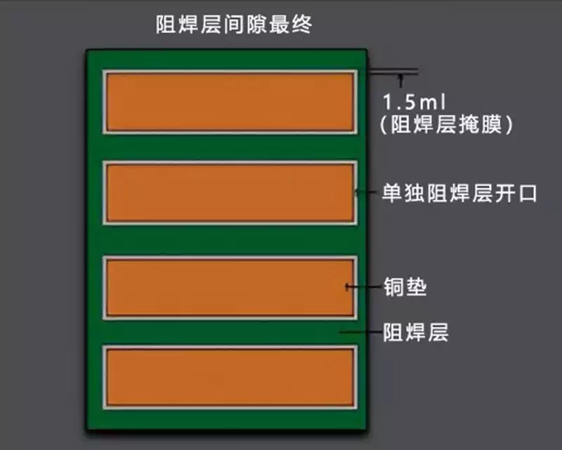
Why soldermask open size is larger than the line pad size
Typically, the area of the soldermask open is larger than the area of the line pads.If the area of the soldermask opening is the same as the area of the pad, then during the PCB manufacturing process, due to the existence of tolerances,it is possible to cause the soldermask green oil (soldermask) to accidentally cover the pad. Therefore,in order to cope with process deviations during PCB manufacturing, we usually need to expand the area of the soldermask window by a certain size. Depending on the production tolerances of most PCB manufacturers, it is generally recommended to expand the soldermask windowing area by 4-6 mils overall.

What should I pay attention to when designing the window?
When designing the PCB bottom soldermask open,you need to pay attention to the following points:
- The size and location of the window should be compatible with the size and location of the components to avoid affecting the installation and welding of components.
- In the PCB process,the design of the open window should take into account the line width and spacing used to extrude the solder paste and spray plating,to avoid the open window part can not be welded.
- Window design should also take into account the thickness of the soldermask layer, to avoid the window after the soldermask layer is too thin, affecting the mechanical strength of the PCB board and the ability to protect.
Soldermask opening role
Soldermask opening refers to the need to weld electronic devices on the window,the unwanted soldermask removal, the formation of a welding device will be exposed to a small area. Soldermask windowing can play the following roles:
- Improve the quality of welding: soldermask opening can reduce the heat of welding to prevent excessive concentration of heat leading to component damage, thereby improving the quality and stability of welding.
- Improve the mechanical strength of the circuit board: Soldermask opening can reduce the thermal and mechanical stress on the circuit board, thereby improving the mechanical strength of the circuit board and reducing the damage rate of the board.
- Improve soldering efficiency: Soldermask opening can reduce the viscosity of the soldering device, improve soldering efficiency and reduce operating time.
- Cost savings: Soldermask opening can reduce the use of materials and processes, thereby saving costs.
PCB soldermask open for ensuring the quality of welding, improve circuit performance and reduce costs is critical. Reasonable design of the window is to ensure that the quality of the finished PCB is a key part of the quality.


