In the manufacturing process of modern electronic products, the manufacturing of printed circuit board assembly (PCBA) is undoubtedly one of the core links. From a bare PCB bare board, to eventually become a feature-rich, stable performance of the core components of electronic products, PCBA manufacturing process is full of precision and efficiency.
From the PCB bare board to the finished PCBA manufacturing steps
1.PCB bare board pretreatment: appearance and clean double guarantee
The first step is to implement a comprehensive PCB bare board appearance inspection, the use of high magnification. Optical detection equipment and other tools, strict reference to the design specifications, check whether the line is broken. Short circuit, whether the copper foil is damaged, whether the hole is smooth. Any minor defects should not be taken lightly, as they may pose major risks for subsequent processing or product use. Subsequently, the use of professional cleaners, follow the chemical cleaning process, thoroughly remove the PCB surface oil. Dust and oxides, to ensure that the subsequent processing of the material can be tightly attached to prevent false soldering. Poor contact and other problems.
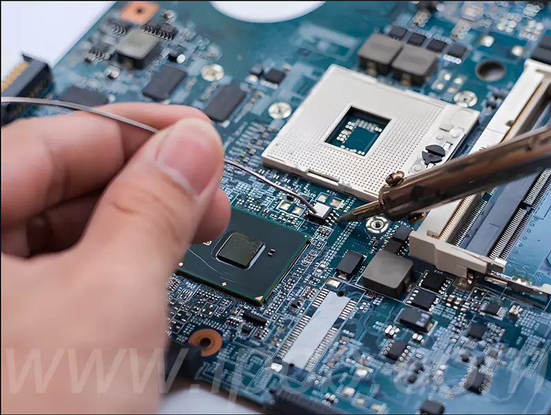
2.Component placement: the key link of precision and efficiency
Accurate preparation of components according to the BOM, to ensure that the type. Specification. The number of components is correct, SMD components are well-packed, and the pins are not deformed. According to the characteristics of components and PCB layout, fine-tuning the parameters of the mounter to ensure stable and accurate placement. Reflow soldering, strict control of the temperature curve to ensure that the heat is evenly transmitted, the solder paste is fully melted and solidified, the formation of reliable solder joints.
3.Plug-in installation: dual consideration of technology and quality
Before plug-in, then check the PCB plug-in holes to ensure that the hole diameter. Hole wall quality up to standard. Manual insertion, the operator needs to strictly follow the process drawings to ensure that the components are accurately inserted, the depth is moderate. Wave soldering, co-adjustment of furnace temperature. Wave height and transfer speed to ensure that the welding is solid. For some components that can not be mounted by SMT technology, such as large connectors, electrolytic capacitors, etc., it is necessary to carry out DIP plug-in processing and manual welding. This includes the components of the plug-in, wave soldering and, if necessary, manual patch welding and other steps.
4.Testing and debugging: double verification of performance and functionality
The use of professional electrical testing tools, such as ICT (in-circuit testers), multimeters and oscilloscopes, etc., the implementation of a comprehensive assessment of the electrical performance of the PCBA. This process involves a circuit-by-circuit conductivity check, verification of signal integrity and distortion-free transmission, and precise measurement of the supply voltage to each functional module. Through exhaustive investigation, potential electrical faults are identified and eliminated in a timely manner, ensuring stable operation of the product after power-up and avoiding unforeseen circumstances such as ‘short-circuit tripping’.
In terms of functional verification,we simulate the actual use of the product in depth, and conduct a full range of functional tests on the PCBA. Taking the motherboard of a smartphone as an example, we will test its communication performance in a variety of network environments, the stability of multi-tasking, and the sensitivity of various types of sensors to changes in the environment. Only after such a rigorous field test, we can ensure that the performance of the product is stable and reliable, stand the test of the market, and ultimately feel at ease to hand over the product to consumers.
5.Final Inspection and Packaging
The last step is to carry out the final inspection and packaging. At this stage, the PCBA will be checked for appearance, performance and safety; to ensure that the product meets the specified standards and requirements. After passing the inspection, the product will be properly packaged to protect it from damage during transport and storage.
From the initial PCB bare board pre-processing, to component placement, plug-in installation, and then testing and debugging, each step of the manufacture of wisdom and sweat. Now, these carefully crafted PCBAs not only meet the most stringent quality standards, but also show excellent performance and functionality.