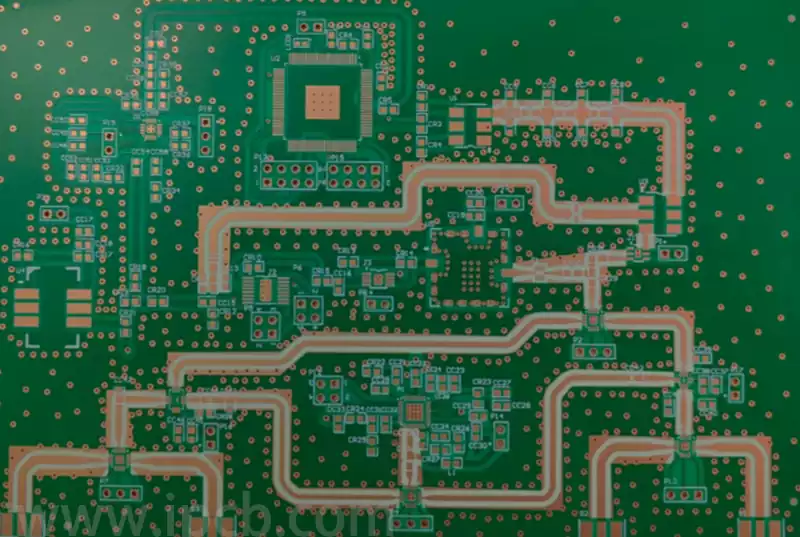
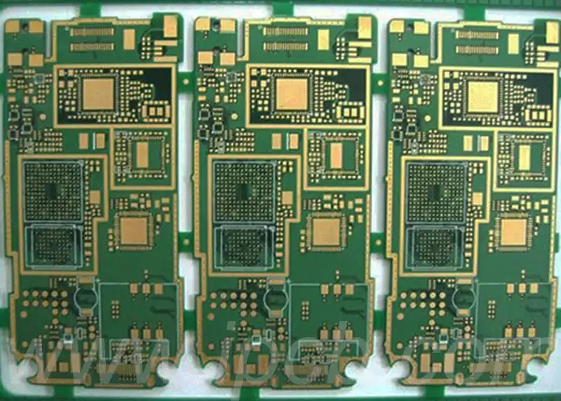
PCB circuit boards are divided into single-sided, double-sided and multilayer type, which the number of layers of multilayer boards are not strictly limited, there are more than 100 layers of PCBs have been introduced, but four-layer and six-layer boards are more common. Many people will be puzzled, why the PCB multilayer board commonly used in double layer design?
1.Cost considerations
From the cost point of view of analysis, although the single-layer PCB due to a layer less media and foil, the cost of raw materials is slightly lower than the double-layer PCB, but its processing costs are significantly higher than the double-layer PCB. in the processing of the inner layer, the cost of the two are similar, however, the foil / core structure of the processing of the single-layer PCB makes the outer layer of the cost of processing a substantial increase. Single-layer PCBs require a non-standard laminated core bonding process in addition to the core structure process. Adding foils to the outside of the core structure reduces factory productivity compared to the core structure. In addition, before the laminated bonding, the outer core also needs additional processing, which not only increases the risk of scratches on the outer layer, but also raises the possibility of etching errors, which in turn pushes up the overall processing costs.
- Prevent bending, quality assurance
Avoid the use of odd-layer design in the PCB circuit boards of a core reason is that odd-layer circuit boards are prone to bending phenomenon. As the layers are bonded and cooled, the difference in lamination tension between the core structure and the foil structure causes the PCB circuit board to flex. As the pcb circuit board thickness increases, so does the risk of bending of the composite PCB, which is a combination of two different structures. The key to ensuring that the pcb circuit board does not buckle is to achieve a balanced laminate structure. Although some degree of bending may still be within specification, this reduces the efficiency of subsequent processing, which in turn drives up costs. At the assembly stage, special equipment and processes are also required to deal with this type of bending, which not only reduces the accuracy of component placement, but also adversely affects the quality of the product.
For example, in the PCB manufacturing process, four-layer boards show a higher degree of control in maintaining symmetry than three-layer boards. The warpage of a four-layer board can be tightly controlled to less than 0.7% (meeting the IPC600 standard), whereas for larger three-layer boards, the warpage is likely to exceed this standard. This warpage not only interferes with the SMT placement operation, but also weakens the reliability of the entire product. Therefore, designers often tend to avoid designing single-layer boards. Even if, functionally, an odd-layer design is sufficient, they still tend to adopt a pseudo-even-layer design, e.g., adjusting a five-layer design to a six-layer one, or a seven-layer design to an eight-layer board, to ensure the stability of the product and the controllability of the manufacturing process.
When a design is faced with an odd-numbered-layer PCB, how do you balance the layer structure, reduce costs, and prevent flexing? Here are a few effective solution strategies:
Add a signal layer: If the PCB circuit board has an even number of power layers and an odd number of signal layers, this strategy can be used. By adding an additional signal layer, not only does it not add extra cost, but it also speeds up the production schedule and improves the overall quality of the PCB circuit board.
Add an additional power layer: This method can be considered when the PCB circuit board has an even number of signal layers and an odd number of power layers. The specific approach is to add a ground layer in the middle of the laminated structure without changing other settings. The wiring is first routed according to the rules for an odd-numbered layer PCB, then the ground layer is duplicated at the middle position and the remaining layers are labelled. This practice is comparable in electrical performance to thickening the ground layer with foil.
Inserting a blank signal layer: In the position near the centre of the PCB layer stack structure, inserting a blank signal layer can effectively reduce the problem of layer stack imbalance, thus improving the quality of the PCB circuit board. The specific operation is: first according to the odd number of layers for wiring, and then insert a blank signal layer in the appropriate location, and mark the remaining layers. This method is especially suitable for microwave circuits and mixed media circuits with different dielectric constants.
As a result, PCB circuit boards design tend to favour an even number of layers to reduce costs and avoid flexing, while odd-layer designs strike a balance through strategic adjustments to ensure manufacturing efficiency and product quality.