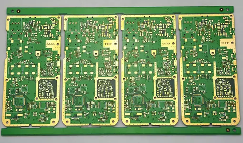
Solder Joint Pillow, also known as the pillow effect (Head-in-Pillow, HIP), is an undesirable phenomenon in which the solder balls of BGAs, CSPs and other components fail to fully fuse with the solder, resulting in the failure to form good electrical connections and mechanical solder joints. This phenomenon is similar to the shape of a person’s head resting on a pillow, hence the name.
Pillow effect (Head-in-Pillow, HIP) is mainly used to describe the circuit board BGA parts in the soldering (Reflow) in the high temperature process, BGA carrier board or circuit board because it can not stand the high temperature and the board bending, board warpage (warpage) or other reasons for deformation, so that the BGA of the ball and the paste printed on the circuit board separation, when the circuit board after the high temperature soldering area temperature gradually drop cooling, then the IC carrier board and the amount of deformation slowly returned to the pre-distortion condition (sometimes not back), but then the temperature has long been lower than the ball and the paste to separate. When the circuit board after the high-temperature soldering area after the temperature gradually drop cooling, then the IC carrier board and the amount of deformation of the circuit board also slowly return to the deformation of the former situation (sometimes can not go back), but then the temperature has long been lower than the tin ball and paste of the melting temperature of the tin, that is, the tin ball and the paste has long since the molten state of the condensation back to the solid state again. When the BGA carrier board and circuit board warpage slowly return to the shape before the deformation, has turned back to the solid state of the solder ball and solder paste again in contact with each other, so the formation of a head on a pillow similar to a false soldering or false soldering of the shape of the solder.
Pillow effect (Head-in-Pillow, HIP) although characterised as a reflow soldering process interface soldering defects, but its formation mechanism is really a multi-dimensional process chain out of control of the composite results, involving PCB substrate, BGA / CSP components, paste materials, equipment precision, process parameters and environmental control and other variables of the whole process. From the human – machine – material – law – ring quality control system analysis, its potential causes can be summarised as the following core links of synergistic failure:
Stencil process design defects: stencil opening geometric parameters (such as area ratio <0.66, aspect ratio >1.5) deviate from the IPC-7525 standard, resulting in insufficient solder paste release rate or bridging risk, solder paste deposition on the pad surface deviation exceeds ± 20%, forming a regional solder coverage of the void;
Printing process parameters mismatch: squeegee pressure, printing speed, demoulding speed and other parameters do not match the rheological properties of the solder paste (thixotropic index of 3-5), resulting in a solder paste transfer rate of less than 85%, the edge of the pad appeared in the solder paste collapsed or concave, the formation of asymmetric wetting interface;
Loss of control of placement positioning accuracy: when the Z-axis pressure fluctuation of the placement head is >±0.05N, and the repeat positioning accuracy of the visual alignment system is <±25μm, the offset between the component solder ball and the centre of the pad is more than 20% of the diameter of the solder ball, which results in the solder not being able to completely wrap the intermetallic compound (IMC) layer; Substrate thermal deformation instability: PCB in 230-260 ℃ reflow peak temperature occurs Z-axis warpage > 0.75% (IPC-TM-650 standard), or BGA / CSP package body due to the CTE mismatch (substrate and chip CTE difference > 3ppm / ℃) bow deformation, resulting in the solder ball and the solder paste contact surface radius of curvature deviation of more than the diameter of the ball of solder ball 15 per cent;
Abnormal decay of solder paste activity: flux system rosin-type active agent (R / RA type) boiling point is lower than 200 ℃, in the preheating zone (150-180 ℃) that is the occurrence of thermal decomposition, resulting in the removal of oxide film ability to decline by more than 40%, the surface tension gradient imbalance in the melting of the solder;
Thermal cycling parameters out of order: reflow time of more than 120 seconds or peak temperature > 260 ℃, the solder alloy (such as SAC305) excessive remelting occurs, IMC layer thickness from 1-3 μm abnormally thickened to more than 5 μm, resulting in an increase in interfacial brittleness and flux volatility;
DFM design compatibility defects: PCB pad design does not follow the IPC-7351 standard (such as pad diameter < 80% of the diameter of the solder ball), or the implementation of the J-STD-033 specification control of MSD (moisture-sensitive devices), resulting in moisture absorption after the popcorn effect triggered by interface delamination.
The superposition of the above factors, ultimately leading to the solder ball and solder paste in the molten state only to form a point contact rather than surface contact, the solder joint cross-section shows a typical ‘headrest’ morphology (IMC layer thickness <0.5μm and distribution intermittent). As electronic products evolve towards high density and high reliability, the quality bottleneck of the head-in-pillow (HIP) effect needs to be systematically solved through a combination of DOE experimental design to optimise the process window, the use of laser-cut stencils to improve printing accuracy, the introduction of closed-loop control of placement pressure by machine vision, and the development of lead-free solder pastes with low void rates.

How to detect bad BGA HIP (Head-In-Pillow) soldering?
Most of the HIP (Head-In-Pillow) effect should occur at the edge of the BGA parts, especially the four corners of the position, because the warpage there is the most serious, if so, you can try to use a microscope or fibre-optic endoscopy to observe, but usually this can only be seen in the outermost two rows of solder balls, and then inward will be very difficult to identify, and so the observation of the BGA solder balls also have to make sure that the side of the high parts are not blocking the view, with the current high-density design of circuit boards, there are many restrictions on the implementation. With the high density design of the current circuit boards, there are many limitations to the implementation.
In addition, the pillow effect (HIP) can now be found using 2.5 D X-Ray inspection machine, and in some cases can also be detected by in-circuit test (ICT, In Circuit Test) and functional test (FVT, FunctionVerification Test), because these machines usually use a needle bed operation, the need to add additional external pressure on the board. Additional external pressure on the circuit board, so that the original next to each other, the solder balls and solder paste have the opportunity to separate, but there will still be defective products flow to the market, usually this kind of defective products will soon be found by the customer has functional problems and was returned, so how to prevent the occurrence of the pillow effect of the SMT for the important issues.
At present, the more reliable way to analyse HIP defects is to use Dye Penetration and Cross Section analysis, but these two methods are destructive, so it is not recommended to use them unless necessary.
For HIP (Head-In-Pillow) failure mode of the root cause – PCB substrate and IC carrier board in the high temperature reflow stage of non-linear warpage deformation, based on ‘material strengthening’ and ‘process compensation’. ‘process compensation’ two technical paths to build a systematic solution, the specific implementation strategy is as follows:
- Material rigidity upgrading strategy
Through the use of high glass transition temperature (Tg) plate to enhance the thermo-mechanical stability of the substrate, it is recommended to use Tg ≥ 170 ℃ high-performance FR-4 materials (such as Lianmao IT-180A, SangYi Technology S1170), the resin system through the introduction of the introduction of cyanoacid ester (CE) or bismaleimide (BMI) modification, so that the substrate in the peak temperature of the reflow of the substrate in the peak temperature of the Z-axis expansion coefficient (CTE) reduced to 40ppm / 40ppm / 260 ℃ reflow temperature. ) is reduced to below 40ppm/°C, a 30%-40% reduction in thermal deformation compared to conventional Tg150°C sheets (CTE 55-65ppm/°C). It should be noted that this solution will lead to material cost increase of 15% -25%, and the need to support the upgrading of the lamination process (pressure ≥ 500psi, vacuum ≤ 5mbar) in order to avoid residual stress in the plate. - Solder paste compensation filling strategy
Dynamic solder paste volume control technology to balance the solder filling and short circuit risk, specific measures include:
Stencil aperture optimization: BGA pad implementation of the ‘main pad + anti-bridging ring’ composite aperture design, the main pad diameter than the diameter of the solder ball is reduced by 5% -8% (such as 0.4mm solder ball corresponds to 0.36-0.38mm pad), anti-bridging ring width of 0.05-0.08mm, through the laser cutting stencil (thickness of 0.12mm) to achieve solder paste filling and short circuit risk. 0.12mm) to achieve solder paste deposition deviation <±10%;
Gradient printing control: in the BGA area using a secondary printing process, the first layer of printing using Type4 (5-15μm) fine powder solder paste to form the base solder joint skeleton, the second layer of printing Type5 (3-8μm) ultra-fine powder solder paste to fill the micro-gap, the total printing height control in the solder ball diameter of 60% -70%, with nitrogen protection (O₂ concentration <500ppm) to inhibit the generation of oxide film;
Real-time monitoring and early warning: deploy the machine vision system to 3D detect the volume of solder paste after printing (accuracy ± 0.01mm³), when the volume of solder paste deviates from the theoretical value of ± 15% triggers the dynamic compensation of process parameters (squeegee pressure ± 0.03N, printing speed ± 5mm / s).
- Mechanical support constraint strategy
PCB three-dimensional thermal deformation suppression through customised carriers, the core scheme includes:
Rigid tray design: 3mm thickness aluminum alloy (6061-T6) or carbon fiber composite material is used to make the tray, and the surface is set up with PCB shape-matching locating tabs (height 0.2-0.3mm) and vacuum adsorption holes (aperture Φ0.8mm, spacing 15mm), together with the reflow oven guideway pressure system (0.2-0.4MPa) to control the amount of PCB warpage at 0.15 within 0.15mm;
Local Pressurisation Module: Configure programmable pressure claw mechanism for BGA encapsulation area, applying 0.1-0.2N vertical pressure in the preheating zone (150-180℃), and raising the pressure gradient to 0.3-0.5N in the reflow zone (210-250℃) to ensure that the contact rate between the solder ball and the solder paste is >95%;
Dynamic simulation verification: use ANSYS Workbench software to carry out thermal-force coupling simulation of the carrier-PCB system, optimise the layout of the support points (recommended support point spacing ≤ 100mm) and the pressure distribution curve, so that the maximum principal strain of the PCB is reduced by 60%-75% compared with the unsupported state.
The prevention and control of HIP failure need to run through the material selection, dynamic optimisation of process parameters and mechanical constraints on the design of the whole process of collaborative innovation, through the establishment of the ‘material – structure – process’ trinity of quality control system, can systematically reduce the HIP defect rate to 0.05% or less of the industry benchmark level. In the future, with the popularity of SiP/3D packaging technology, HIP failure mechanism will evolve to the micro-nano-scale thermal coupling direction, need to continue to deepen the material CTE matching, transient thermal deformation simulation and AI-driven adaptive control of the process and other cutting-edge technology research, high-density electronics manufacturing for building a solid foundation of reliability.