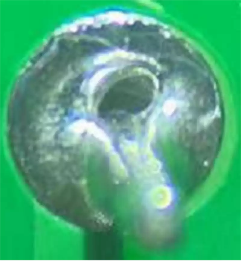
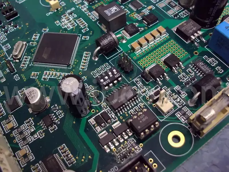
Ion cleanliness typically refers to the ion cleanliness of pcb board. Residual ions from various materials during the cleaning process can compromise the functionality and reliability of electronic products. Common issues arising from ionic contamination include surface corrosion and crystalline growth, ultimately leading to short circuits. Excessive current flow through connectors may result in the eventual failure of electronic devices.
Several contaminants primarily originate from processes such as electroplating, wave soldering, reflow soldering, and chemical cleaning. These include five main forms: flux residues, ionised surface activators, ethanol, aminoethanol, and human perspiration.
Consequently, conducting ion cleanliness testing to identify contaminant sources and reduce product defect rates is becoming increasingly vital for enterprises.
Five Common Methods for Testing Ion Contamination Levels in PCBA:
- Ion Chromatography (IC) Testing: This method accurately determines the types and concentrations of anions, cations, and organic acids present on PCBs. The sample is first immersed in a specific ratio of isopropanol and water solution to dissolve contaminants, followed by analysis using an ion chromatograph.
- ROSE Testing: ROSE (Solvent-Extracted Resistivity) is a traditional ion contamination assessment method. It evaluates contamination levels by measuring the conductivity or resistivity of PCBs in specific solvents. Although once widely used, the IPC organisation now considers its predictive capability for ion contamination levels to be insufficient.
- Surface Insulation Resistance (SIR) Testing: This method evaluates cleaning efficacy by measuring the surface insulation resistance between conductors on the PCB assembly. It enables direct, quantitative analysis of contamination, proving particularly suitable for hard-to-clean areas such as BGA solder joints.
- NaCl Equivalent Method: This technique indirectly reflects total ionic contamination by measuring solution conductivity. During operation, the PCB is first cleaned with a specific solution. The resistivity of the post-cleaning solution is then tested, with results expressed as NaCl equivalents per square centimetre.
- Particle size and count method: A relatively novel cleanliness assessment technique. It evaluates cleanliness by microscopically observing the size and quantity of contaminant particles on filter membranes.
Common Cleanliness Testing Standards
Testing Standards
PCB surface cleanliness testing is typically determined by customer requirements and industry specifications, such as the IPC-5702 standard. IPC-5702 is a circuit board cleanliness testing standard established by the International Electronics Manufacturing Alliance (IPC), primarily used to assess PCB cleanliness. The IPC-5704 standard specifically addresses cleanliness requirements for unfilled printed circuit boards, aiming to prevent or remove ionic contamination and other unwanted debris. Additionally, Section 3.9 of IPC-6012 establishes PCB cleanliness standards, such as limiting contamination to no more than 1.56 µg/cm² of NaCl equivalent. The IPC standard for clean boards requires ionic test results below 6 µg NaCl equivalent per square inch. Within the automotive components sector, the ISO 16232 cleanliness testing standard imposes standardised requirements for PCB board cleanliness testing procedures and particle detection in accordance with this specification. The VDA 19.1 document issued by the German Association of the Automotive Industry clearly defines the technical cleanliness of automotive components and provides multiple methods for testing and enhancing cleanliness, establishing itself as a widely followed standard within the automotive sector. Commonly used standards for ionic contamination analysis also include IPC-TM-650 2.3 28B, which specifies requirements for detecting seven common anions and eight weak organic acids.
Testing Equipment
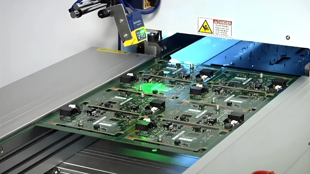
Automated optical inspection (AOI) technology finds extensive application in industrial PCB testing, such as during the reflow process of printed circuit boards (PCBs). Its fundamental principles encompass optical imaging methods, key system integration technologies, image processing, and defect classification methodologies. The C3 tester can be employed to verify contamination levels in specific areas and identify contamination sources, particularly when contamination exceeds specified limits. For online automated detection systems of PCB surface defects, key technologies requiring overview include visual illumination techniques, large-field-of-view high-speed imaging, distributed high-speed image processing, precision transmission and positioning, and networked control systems. Previous PCB surface cleanliness requirements no longer meet current product demands, consequently raising standards for total ionic contamination and specific ionic contaminants (e.g., Na, Cl, Br, SO₄).
Personnel Training
Professional training for PCB cleanliness inspectors is paramount to enhance their detection skills and proficiency. Technical engineers should conduct training for frontline production technicians, particularly regarding PCB ionic cleanliness testing protocols. Additionally, operators of wastewater treatment facilities must undergo role-specific skills training. Achieving a comprehensive understanding of rigid PCB design, specifications, manufacturing, and inspection will foster product consistency, deepen grade comprehension, and yield higher, more reliable product quality.
The Importance of PCB Cleanliness Testing
- Enhancing Product Reliability: During production and assembly, PCB boards may retain contaminants such as solder dross, flux residues, and dust. If not promptly removed, these contaminants can cause circuit short-circuits, signal interference, and other issues, severely impacting product functionality and lifespan. Cleanliness testing enables timely detection and removal of such contaminants, ensuring product reliability.
- Enhancing Product Aesthetics: As consumer expectations for electronic product appearance rise, PCB cleanliness directly impacts overall product presentation. A clean, tidy PCB not only improves visual appeal but also bolsters consumer confidence in product quality.
- Safeguarding Production Safety and Environmental Protection: Certain contaminants remaining on PCBs may pose risks to human health and the environment. Cleanliness testing enables the timely identification and management of these potential hazards, ensuring both the safety and environmental sustainability of the production process.
PCB board ionic cleanliness testing is a critical step in ensuring the functionality and reliability of electronic products. Cleanliness not only directly impacts a product’s electrical performance and long-term stability but also profoundly influences its visual quality, consumer satisfaction, and the safety and environmental sustainability of the production process. Looking ahead, as electronic products trend towards miniaturisation, higher integration, and enhanced performance, demands on PCB cleanliness will become increasingly stringent. Continuously optimising testing techniques, introducing more intelligent detection equipment, and strengthening collaborative standards across industries will be pivotal to ensuring electronic products maintain exceptional performance and longevity even in complex environments.