The encapsulation process, also known as the packaging process, involves the secure enclosure of semiconductor chips using specific materials. This provides effective defence against environmental degradation, ensuring stable chip operation. Beyond delivering crucial physical protection, the process is designed from the outset to fully account for the inherent characteristics of chips – namely their lightweight, thin, compact and miniature nature. It strives to maintain and optimise these advantages while providing safeguarding.
This critical step constitutes an indispensable component of the semiconductor manufacturing process. By integrating exposed chips into protective encapsulation structures, it effectively shields them from potential threats such as moisture, dust, chemical agents, and mechanical stress. The selection and design of encapsulation directly influence chip reliability, performance characteristics, and ultimately the dimensions and cost of the finished product.
In essence, the encapsulation process is a precision engineering endeavour. By enclosing the semiconductor chip within a protective shell, it not only preserves its ‘lightweight, thin, compact, and small’ attributes but also ensures the chip achieves the required electrical connections and thermal dissipation across diverse operating environments, thereby extending its operational lifespan.
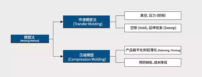
The encapsulation process is broadly categorised into two methods: sealing and moulding. Hermetic sealing typically involves attaching ceramic plates or metal caps to achieve sealing. In contrast, moulding entails melting plastic epoxy materials before curing them to form a seal. Currently, hermetic sealing is relatively less common, while moulding—particularly using epoxy resin moulding compounds—is more prevalent. For resin-filled semiconductor methods, moulding can be further subdivided into transfer moulding and compression moulding.
Hermetic Sealing
Hermetic sealing employs ceramic plates or metal covers to encapsulate semiconductor devices, providing physical protection. This method aims to create an airtight environment shielding the chip from external factors such as moisture and oxygen. Whilst historically utilised, this approach is now less common.
Hermetic sealing offers exceptional reliability but is costly. Consequently, moulding techniques employing epoxy moulding compounds (EMC) are predominantly adopted. With continuous improvements in plastic raw materials—addressing issues like moisture content and internal voids—the application scope of plastics is expanding rapidly. For EPROMs, plastic materials are employed for sealing in virtually all instances. Furthermore, most packaging solutions utilise plastic materials, encompassing dynamic random-access memory (DRAM), central processing units (CPUs), and NAND flash memory.
Moulding material: Epoxy Moulding Compound (EMC)
As a plastic material, Epoxy Moulding Compound (EMC) serves as one of the fundamental functional materials required for semiconductor back-end processes. EMC primarily consists of resin-based materials, supplemented by fillers and curing agents. When powdered epoxy resin melts and dissolves into a gel state at 175°C, its viscosity decreases. Upon cooling, the epoxy resin cures, with viscosity increasing inversely with temperature. As temperature further decreases, the epoxy resin bonds firmly to surrounding components such as printed circuit boards (PCBs), lead frames, wires, and wafers, transforming into an extremely hard material. This material is termed thermosetting epoxy resin. Crucially, once cured, the EMC expands and contracts in tandem with the chip when temperature fluctuations occur during semiconductor operation. Additionally, this material facilitates efficient heat dissipation externally, which is equally vital. Thus, the properties of this composite material fundamentally determine the reliability of the EMC.
Moulding Process Types
Moulding involves shaping an object into a specific form. During semiconductor moulding, the encapsulant material is melted and injected into a cavity. The tool responsible for shaping is pivotal to the moulding process, namely the moulding plate. Moulding methods encompass transfer moulding (an older technique), vacuum compression moulding (an improved method addressing transfer moulding’s shortcomings), and compression moulding (vertically oriented towards the substrate).
Transfer Moulding
Transfer moulding is an earlier moulding technique primarily employing resin materials. In this process, epoxy resin is melted to a gel state and then forced through multiple narrow channels by applying pressure (i.e., ‘poured’). However, as chip dimensions continue to shrink, layer counts increase, and wire bonding structures grow increasingly complex, achieving uniform resin distribution during moulding becomes challenging. This may result in incomplete moulding or an increase in voids (or porosity). In other words, precisely controlling the flow rate of the epoxy resin becomes significantly more difficult.
To address these challenges, researchers have developed an improved method: as the epoxy resin flows through the narrow channels, a vacuum is formed on the opposite side and drawn out, effectively controlling the resin’s flow rate. Furthermore, the industry is actively exploring various methods to reduce voids, ensuring the epoxy resin spreads uniformly and fills all intricate structures.
Compression Moulding
As chip layer counts increase (e.g., in multi-chip packages, MCP) and wire bonding complexity rises, the limitations of transfer moulding become increasingly apparent. Particularly driven by cost reduction, the dimensions of carriers (such as printed circuit boards or lead frames) continue to grow, making transfer moulding more challenging. With epoxy struggling to penetrate and uniformly spread within increasingly intricate structures, the industry urgently requires a new moulding technique.
Compression moulding emerged to address these limitations. In this process, the epoxy moulding compound (EMC) is directly placed within the mould for melting, eliminating the need for long-distance transfer of the resin. The critical step in compression moulding involves vertically positioning the wafer to be encapsulated directly onto the gel-like epoxy resin. This vertical placement and direct compression significantly reduce defects such as voids and tension. Furthermore, the method is more environmentally friendly due to reduced unnecessary epoxy resin usage.
Currently, both transfer moulding and compression moulding remain concurrently employed in semiconductor packaging. However, compression moulding is increasingly favoured by suppliers due to its advantages in defect detection, cost-effectiveness, and environmental sustainability. With the sustained growth in customer demand for flatter, thinner, and lighter products, compression moulding is anticipated to see broader and more active application in the future.
Comparison and Advantages/Disadvantages of Two Moulding Methods
| Characteristics | Transfer Moulding | Compression Molding |
| Principle | Pressure-inject the pre-melted epoxy resin into the mould cavity and cure it | Place the EMC directly into the mould, heat it to melt, then apply pressure to cure it |
| Scope of Application | Suitable for conventional packaging, but with limitations for complex structures and large carriers | More suitable for multi-chip packages (MCP) and complex structures, particularly in advanced packaging where thinness, lightness and high reliability are required |
| Defect control | The long flow path of epoxy resin readily leads to the formation of voids and uneven flow distribution | Direct compression reduces the flow of epoxy resin, thereby minimising defects such as voids and shrinkage |
| cost | Moulding costs are typically high and may necessitate additional equipment such as vacuum assistance | Mould costs are relatively low, and the production process is relatively straightforward |
| Environmental impact | Material wastage may occur due to epoxy resin migration | By reducing unnecessary epoxy resin usage, it is more environmentally friendly |
| Trends in Development | Faced with challenges from emerging technologies, its application has gradually declined | Owing to its advantages and adaptability to advanced packaging, it is anticipated that it will see wider application in the future |
| Accuracy | High precision, good surface finish | More suitable for large thick-walled components |
| Process complexity | Rubber moulding method: Preformed thermosetting polymer is placed within a vessel, heated and pressurised to flow into a closed cavity | Rubber introduction method into the mould: The rubber is placed directly into the mould cavity, then compressed and heated to form the part |
The encapsulation process is central to semiconductor manufacturing, designed to protect the chip and optimise its characteristics of being lightweight, thin, compact and small. The continuous evolution of packaging technology, particularly innovations in moulding processes, ensures semiconductor chips deliver superior performance and extended service life within ever-advancing electronic products. Moving forward, encapsulation techniques will continue to advance towards greater efficiency, reliability and environmental sustainability to meet the growing demand for miniaturised, high-performance chips.