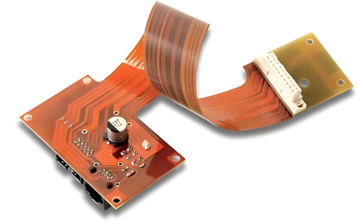
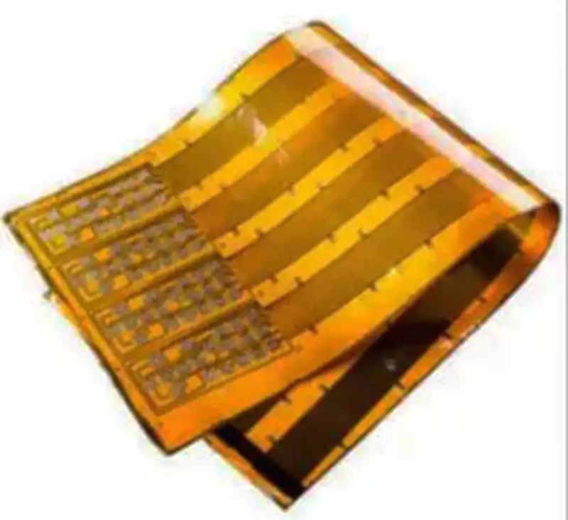
As electronic products accelerate towards lighter, slimmer, smaller and higher-density designs, traditional rigid PCBs struggle to meet specific structural and performance demands. Flexible PCB (FPC), however, shine across numerous sectors including mobile phones, cameras, wearables, medical electronics and automotive electronics, owing to their unique ability to bend, fold and stretch. Particularly in critical areas such as camera modules, OLED displays, and antenna feedline connections, FPCs have become virtually the only viable option.
Unravelling the Manufacturing Principles and Material Structure of Flexible PCBs
The core advantage of flexible PCBs lies in their ability to maintain stable electrical performance while enduring a degree of mechanical deformation. This characteristic is achieved through substrate materials and structural designs that differ fundamentally from those of rigid boards.
Analysis of Fundamental Material Composition
PI (Polyimide) Substrate: Common brands like DuPont’s Kapton offer high thermal resistance, mechanical strength, and excellent flexibility, providing a robust physical foundation for flexible PCBs.
Copper Foil: Categorised into Rolled Annealed (RA) and Electrolytic Doped (ED) copper. RA copper exhibits superior ductility, making it ideal for applications requiring repeated bending.
Bonding Agent: Plays a pivotal role in the lamination process, firmly bonding copper foil to PI. Primarily categorised as imide-based or acrylic-based.
Cover Film: Not only shields circuits from external damage but also provides insulation, typically employing a PI + adhesive structure.
These materials undergo a series of processes—including hot pressing, pattern transfer, and electroplating—to form a complete flexible circuit board. Unlike FR4 rigid boards, every processing step for FPCs is strictly constrained by the material’s deformability.
Classification of Flexible Boards
Single-sided Flexible Board: Features a single circuit layer, offering relatively lower cost and suitability for simple interconnection requirements.
Double-sided Flexible Board: Incorporates two copper layers, capable of meeting moderately complex circuit design demands.
Multi-layer Flexible Board: Achieves three or more layers, suitable for high-density connection scenarios, providing solutions for intricate circuits.
Rigid-Flex Boards: Combine rigid sections with flexible areas, presenting complex structures demanding exceptionally high design precision.
Different flexible board types necessitate distinct manufacturing processes. We shall now examine critical stages in their production.
Analysing Specialised Process Requirements for Flexible PCB Manufacturing
Key Considerations for Pattern Transfer (Circuit Imaging)
Flexible materials lack the stability of rigid boards, making them prone to wrinkling and slippage during processing. Therefore, particular attention must be paid during the pattern transfer stage:
Employ low-tension coating techniques to prevent material stretching and deformation during imaging.
When using exposure equipment, ensure uniform light distribution to avoid material distortion caused by uneven illumination.
Opt for dry film processes, which are more suitable for thin PI materials compared to wet film methods.
Pattern alignment must achieve high precision, particularly in double-sided boards, to prevent misalignment between upper and lower patterns.
Pattern line width and spacing should be designed at ≥75μm; values below this significantly increase yield challenges.
Precautions for Drilling and Electroplating
Laser drilling technology is predominantly employed for FPC drilling, particularly for small holes (e.g., <0.2mm) and blind/buried vias.
Laser-drilled edges must remain clean to prevent charring of the PI material.
Power and pulse width during drilling must be strictly controlled to prevent substrate tearing.
Post-laser-drilled hole walls require activation via plasma or chemical methods to enhance electroplating adhesion.
The copper plating layer must be uniform and sufficiently thick to prevent fractures.
For flexible boards, avoid designing large pads around vias; instead, employ teardrop transitions to prevent tearing.
Methods to Mitigate Manufacturing Issues During Design
Many challenges in flexible PCB fabrication can be effectively avoided during the design phase.
Bending Radius Specifications
Perpendicular bends in traces are prohibited; use arcs or gradual curves instead.
For single-layer PI, the bending radius should be ≥5–10 times the board thickness.
Multi-layer boards require even greater bending radii to prevent internal stress concentration.
Strategies to Avoid Repeated Bending Areas
Avoid routing traces in frequently folded regions.
If routing is unavoidable, trace routing should follow the same direction and avoid crossings.
Placing vias or components within flexible bending zones is not recommended.
Key Structural Layout Considerations
Offset via locations from bending zones to prevent crack propagation.
Reinforce pad edges with structures such as cover plates or thickened PI.
When employing ‘gold fingers’ or ZIF connectors, reinforce the gold finger area additionally.
Consider panelisation for manufacturing
Flexible boards should not be manufactured as single sheets; panelisation must be considered.
Support processing using FR4 auxiliary frames or rigid carrier sheets.
Include positioning holes along process edges to facilitate subsequent placement and testing.
Flexible PCBs demand systematic design-manufacturing collaboration
Flexible PCBs are not merely ‘bendable circuit boards’; they represent a distinct material system, process requirements, and design philosophy compared to rigid boards. Every stage—from material selection to process control—requires seamless coordination. Failure at any point may trigger severe consequences like cracking, delamination, or complete failure.
Therefore, producing high-quality flexible PCBs necessitates the joint participation of design engineering, manufacturing engineering, and quality control throughout the entire process. Engineers should communicate relevant manufacturing constraints with the production facility at the earliest design stage to avoid repeated modifications and rework later on. Simultaneously, for products entering mass production, comprehensive process validation must be conducted to ensure the long-term reliability and consistency of the flexible circuit boards.
Looking ahead, as high-density, miniaturised electronics continue to evolve, flexible PCBs will shoulder increasingly complex tasks. Mastering their manufacturing characteristics has become an essential skill for every electronics engineer.