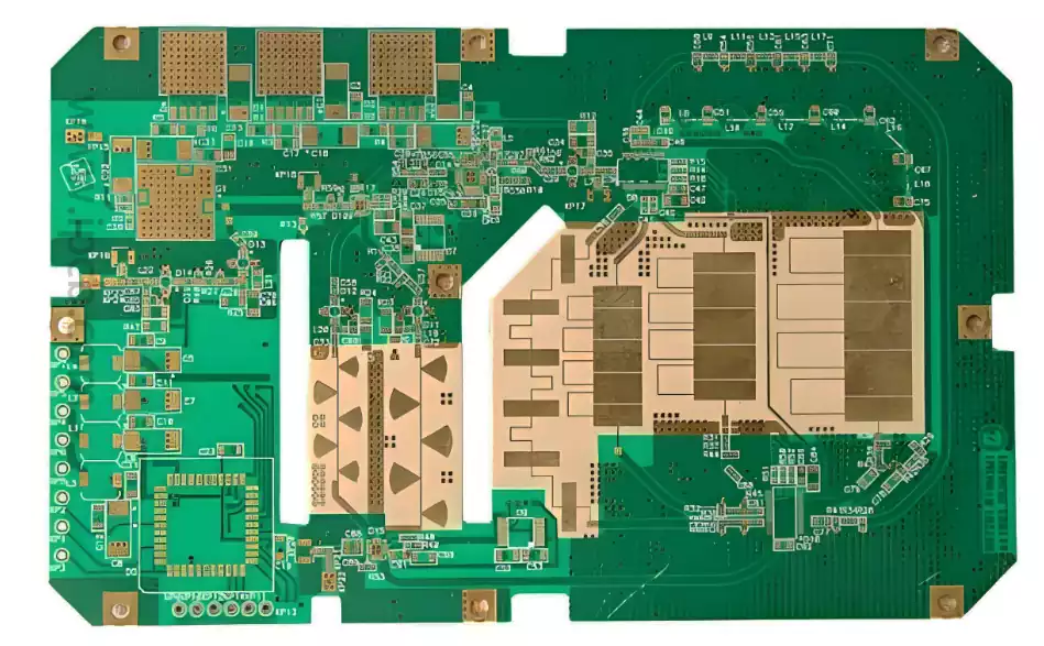
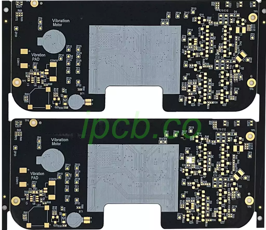
The copper layer on a circuit board serves as a conductive foil, primarily functioning to interconnect electronic components. These components are typically connected to one another or to power circuits via this copper layer, facilitating current and signal transmission throughout the circuit. On the board, the solder joints of component pins connect to other pins or power circuits through this copper layer. Consequently, the quality and layout of the copper layer significantly impact the proper functioning of the circuit board.
The Importance of Circuit Copper Foil in PCB Design
- The Significance of Copper Foil Layout
In PCB design, designers must arrange the copper foil layout rationally to achieve proper connections between circuit components and robust current-carrying capacity. If the copper foil area is too small, connections between components may become problematic, causing the circuit boards to malfunction. Conversely, an excessively large copper foil area wastes valuable board space, thereby compromising the PCB’s overall performance. - Quality Requirements for Copper Pads
The quality of copper pads constitutes another critical consideration in PCB design. Generally, copper pads should exhibit excellent electrical conductivity, machinability, and corrosion resistance. Furthermore, their thickness must be appropriately adjusted according to the power and current load of the circuit components. Substandard copper pads can compromise the performance and reliability of the circuit board, potentially leading to malfunctions.
Causes of Copper Leakage in Circuit Boards
- During PCB fabrication and design, excessive emphasis on enhancing adhesion between copper and other materials may lead to copper layer peeling, incomplete adhesion, or defects due to processing errors or human factors.
- In PCB quality testing, excessive density or inadequate evaluation can also be contributing factors. Excessive vibration or mechanical stress may cause copper to detach or peel.
- Chemical treatment of PCB surfaces is critical. Abnormalities such as improper chemical cleaning or etching conditions, or insufficient processing time, can roughen the protective layer’s surface, compromising copper coverage.
- Non-standard copper plating processes. If internal PCB structure design or hardware systems fail to meet required technical specifications, copper layers may scatter or exhibit persistent adhesion issues.
- Environmental factors constitute another significant cause of PCB copper leakage. During transportation and finished product storage, exposure to natural elements such as humidity or pH levels may cause separation between the protective layer and substrate, resulting in copper leakage.
Hazards of PCB Copper Leakage:
- Compromises circuit stability and reliability. Copper leakage may cause false connections or disconnections, leading to abnormal operations that prevent proper circuit functioning or cause long-term operational issues, thereby affecting product performance and lifespan.
- Metal corrosion undermines the board’s corrosion resistance, resulting in faulty conductors.
- Reduces the service life of the PCB circuit board. Copper leakage may prevent component recognition, thereby shortening the board’s operational lifespan.
- In extreme cases, copper leakage poses safety hazards. Faults or improper operations, such as short circuits, can cause board overheating and explosions.
Solutions for Exposed Copper on Circuit Boards
- Copper foil repair: For small exposed copper areas, copper foil tape or sheets may be applied. Wrap the foil over the exposed copper and gently tap it with a hammer to ensure secure adhesion. Note that the foil must make good contact with the exposed copper to maintain conductivity.
- Repair using additives: Commercially available additives can restore exposed copper. Application is straightforward: apply an appropriate amount to the affected area. Once applied, the additive integrates into the copper, forming a protective layer that prevents further corrosion.
- Re-plating: For extensive copper exposure or corrosion, re-plating is an option. This process involves removing the exposed copper layer and applying a fresh copper coating. This method is suitable for significant copper exposure or severe corrosion.
Copper cladding is critical in PCB design, with its layout and quality directly impacting board performance. PCB copper exposure issues arise from diverse causes and pose significant hazards. However, through the judicious application of copper foil repair, additive treatment, and re-plating, these problems can be effectively resolved, ensuring stable and reliable circuit board operation.