In electronic manufacturing, flexible printed circuits are widely utilised, with HASL being a common PCB surface finishing process. So, is HASL suitable for flexible circuit boards?
HASL, standing for Hot Air Solder Leveling, is an extremely prevalent surface treatment technology within the PCB (printed circuit board) sector. Its core function lies in establishing a uniform layer of tin upon exposed copper surfaces, thereby safeguarding the copper layer from oxidative corrosion and ensuring excellent solderability during subsequent soldering operations.
The operational sequence is straightforward:
The circuit board undergoes thorough cleaning followed by flux application. It is then immersed in a molten solder bath (maintained at 250°C to 265°C). Once the solder fully covers the copper surfaces, two streams of high-temperature, high-pressure hot air are simultaneously directed from above and below. This removes excess solder and smooths the surface, ultimately forming a relatively flat and lustrous tin layer.
The significant advantages of the HASL process are: low cost, making it highly suitable for large-scale batch production; a mature and stable process with extremely widespread availability of related equipment and operational procedures; strong adhesion between the solder layer and substrate, delivering reliable soldering performance. Consequently, HASL stands as one of the most prevalent and economical surface treatment solutions for traditional rigid PCBs (primarily FR-4 material).
However, the HASL process carries a significant ‘side effect’ that cannot be overlooked: the entire treatment subjects the circuit board to high temperatures and intense hot-air impact. For rigid boards made from glass fibre-reinforced FR-4 material, this poses no significant challenge. However, for flexible materials, it may trigger a series of serious issues.
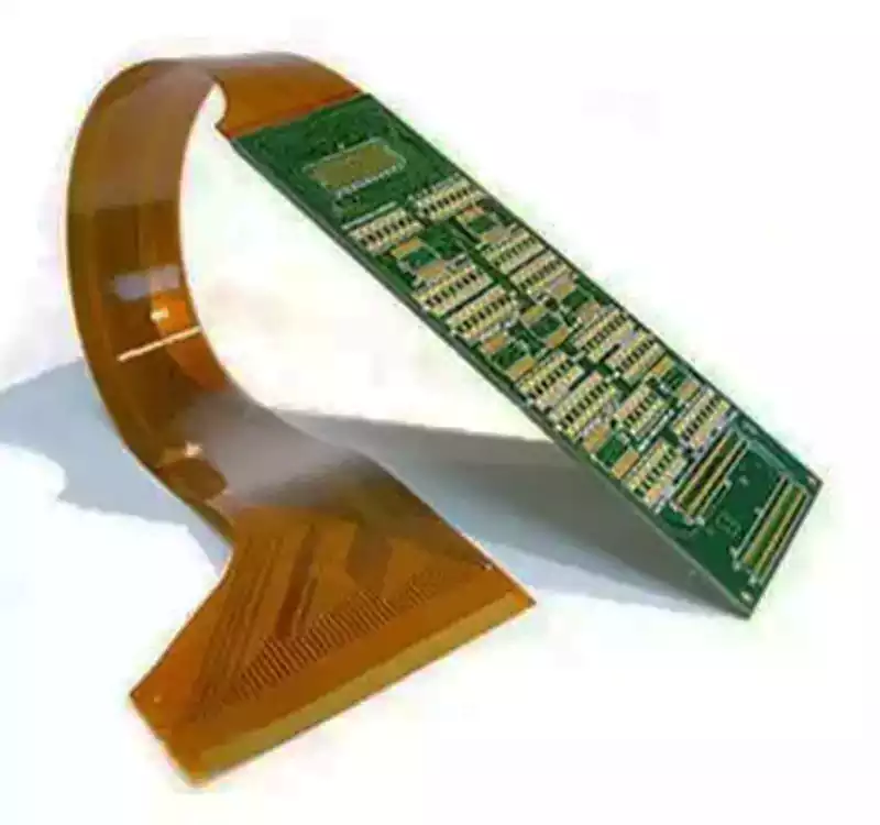
The primary constituent materials of flexible printed circuits are polyimide (PI) or polyester (PET). These materials possess lightweight and flexible properties, though this also implies their heat resistance and mechanical strength are relatively limited.
During HASL, molten solder temperatures routinely exceed 250°C, while hot-air pressure remains substantial. Under such extreme conditions, flexible printed circuits are highly susceptible to noticeable deformation, manifesting as warping, blistering, or even delamination. More problematically, the copper foil thickness on flexible printed circuits is often merely 18μm or even thinner. Their adhesive layer is highly susceptible to softening or delamination under high temperatures. Once delamination or bubbles occur, both the board’s electrical performance and mechanical reliability suffer severe damage. Furthermore, the surface after hot air leveling is not smooth or flat. The HASL process produces an uneven distribution of solder thickness, frequently resulting in ‘solder mounds’ or ‘rippling’ undulations.
Within flexible printed circuits, this leads to variations in pad height, subsequently affecting the placement accuracy of SMT (Surface Mount Technology) and the reliability of solder joints. For components demanding exceptionally high pad flatness (such as BGAs and CSPs), the HASL process is largely incapable of meeting these requirements. Therefore, from multiple perspectives—including material properties, thermal stability, and surface flatness—the HASL process fundamentally conflicts with the requirements of flexible circuit board manufacturing. While theoretically feasible, applying HASL to flexible printed circuits incurs substantial costs and carries significant risks in practical implementation.
Although HASL is unsuitable for flexible printed circuits, this does not imply a lack of superior alternatives for FPCs. In fact, the flexible circuit board industry commonly employs the following surface treatment methods:
Immersion Gold: This is a prevalent surface treatment technique. By immersing the flexible printed circuits in a solution containing gold salts, a uniform gold plating layer forms on the board’s surface. Gold possesses excellent electrical conductivity, corrosion resistance, and solderability, effectively enhancing circuit reliability and stability. It is particularly suitable for high-frequency circuits and microcircuits demanding superior electrical performance. The immersion gold layer presents a flat, smooth surface with excellent solderability, readily bonding with various soldering materials while minimising issues like cold solder joints or bridging during the soldering process.
Immersion Silver: This method involves immersing the flexible printed circuits in a solution containing silver ions, which reduce and deposit onto the board’s surface to form a silver plating layer. The treated surface exhibits excellent conductivity and solderability. Silver’s conductivity is second only to gold, meeting the requirements of most circuits. Moreover, the silver layer forms a stable oxide film in air, providing some oxidation resistance and extending the circuit board’s service life. However, the silver layer is relatively soft and may require additional protective measures in applications involving significant friction.
Electroless Nickel Immersion Gold (ENIG): This process involves first depositing a layer of nickel onto the circuit board surface, followed by a layer of gold over the nickel. The nickel layer provides excellent wear resistance and corrosion resistance, offering mechanical strength and protective properties to the circuit board; the gold layer ensures good electrical conductivity and solderability. This surface treatment combines the advantages of nickel and gold, finding widespread application in electronic devices with high reliability requirements.
Hot Air Solder Leveling (HASL): Molten solder is applied to the surface of a flexible circuit board, then levelled by hot air. The resulting board surface features an even solder layer with good solderability, facilitating subsequent soldering operations. It is cost-effective and suitable for high-volume production. However, the thicker solder layer may compromise the board’s flexibility and high-frequency performance.
Organic Solderability Preservatives (OSP): An organic film is applied to the board surface. This film exhibits excellent stability at room temperature. When soldering is required, heating causes the organic film to decompose, exposing a clean copper surface to achieve good solderability. The OSP treatment is low-cost and simple, suitable for small electronic products with modest electrical performance requirements. However, the organic film exhibits relatively weak corrosion resistance, potentially compromising the PCB’s lifespan in harsh environments.
Surface treatment for flexible printed circuits requires a bespoke approach. While HASL struggles to meet demanding requirements, processes like immersion gold and electroless silver plating each excel in specific areas. Only by precisely matching these techniques to different needs can high-quality flexible circuits be achieved.