The layer of paint on the PCB surface is called solder resist ink, also known as PCB solder mask ink. Solder mask ink is the most common and primary ink used in PCB circuit boards. Typically, 90% of solder resist ink is green, though other colors exist, such as red, blue, black, white, and yellow, which are referred to as miscellaneous color inks.
The function of solder mask ink is insulation. During the soldering process, it prevents short circuits caused by bridging, physical breaks in conductive circuits, and deterioration or corrosion of insulation due to external factors like dust or moisture affecting the traces.
A solder mask bridge refers to the green ink between one component pad aperture and another. It typically denotes the solder mask strip between densely packed IC pin corresponding pads. The function of solder mask bridges is to prevent solder flow during assembly, thereby avoiding component short circuits due to solder bridging. To prevent solder bridging short circuits, maintaining solder mask bridges around pads is essential.
PCB Solder Mask Bridge Process
The manufacturability of solder mask bridges depends on solder mask ink color and copper thickness. Green ink bridges are easier to control than colored inks, allowing for minimal bridge retention. Thicker copper requires larger solder resist bridges, while thinner copper bridges are easier to control.
a. When base copper ≤ 1 oz, ensure solder resist bridges ≥ 4 mil (green and matte green), 5 mil (other colors), 8 mil (only for bridges on large copper planes covering the entire board).
b. For base copper 2-4 oz, solder resist bridges ≥ 6 mil; 8 mil (applies only to solder mask bridges on large copper areas covering the entire board).
c. Between solder mask areas on large copper regions, solder-blocking bridges must be ≥8mil to prevent solder bridging.
PCB Solder Mask Bridge DFM Design
Solder Resist Bridge on Base Material
The size of the solder resist bridge correlates with the IC pad spacing on the circuit layer. Excessively small IC pad spacing may cause solder bridging during component placement. For example: Using green solder mask as an illustration, if the circuit’s IC pad spacing is 8 mil and the pad aperture is 2 mil on one side, the solder mask bridge should be 4 mil. In extreme cases, to preserve the solder mask bridge, the IC pad window can be opened to 1mil on one side. This allows a 4mil solder mask bridge even with a 6mil IC pad spacing.
Solder Resist Bridges on Copper Pads
IC pads on copper pads also require solder resist bridges. Without them, solder wicking into the window would connect adjacent IC pads, effectively merging two pads into one. While this forms a network on the copper layer and avoids short circuits, it compromises component thermal dissipation and complicates rework.
Solder Mask Bridge Width Design Guidelines: Balancing Ink Properties to Avoid Breakage and Failure Risks
Bridge width must be determined by considering “solder mask ink type, PCB layer count, and manufacturing precision.” Excessively narrow bridges risk fracture; overly wide bridges may cover pads, compromising solderability.
Standard Solder Mask Ink (Epoxy Resin Type): Minimum width of 0.1mm to ensure curing strength
The tensile strength of standard epoxy resin solder mask ink after curing is approximately 50MPa. When the width is less than 0.1mm, solder mask bridges are prone to fracture due to stress concentration. Specific requirements are as follows:
Single-sided and double-sided boards: Solder mask bridge width must not be less than 0.1mm.
Multilayer boards (8 layers or more): Due to significant lamination stress and susceptibility to interlayer stress affecting the solder mask layer, higher strength is required. Solder mask bridge width must not be less than 0.12mm.
Flexible solder mask inks (polyimide-based): Width may be moderately reduced to accommodate flexibility requirements.
Solder mask inks used on flexible PCBs must exhibit excellent flexibility, with an elongation at break of no less than 50%. Compared to standard inks, their width may be appropriately reduced by 10%–20%.
For fine-pitch components on flexible PCBs (e.g., FPC connectors): Solder mask bridge width should not be less than 0.08mm to ensure flexibility while preventing breakage.
Solder Mask Bridge Spacing Control Standards: Defining Requirements for Pad and Window Alignment
Solder mask bridges must be precisely positioned. Improper spacing relative to pads or apertures may cause “solder mask covering pads” or “apertures exposing copper foil.”
Solder mask bridge spacing from pads: Minimum 0.05mm to prevent pad coverage
Solder mask bridges must maintain a safety margin from pad edges to avoid ink coverage over pads, which compromises solder quality:
Standard components (0603–1206 size range): Spacing should be no less than 0.05mm.
Fine-pitch components (pin pitch ≤ 0.3mm): Due to tighter spacing, the distance may be appropriately reduced to no less than 0.03mm, but ensure the aperture fully covers the pad.
Alignment precision between solder mask bridges and apertures: Deviation must not exceed 0.02mm to prevent aperture misalignment.
Solder mask bridges must align with aperture edges. Excessive offset causes one side to have an oversized aperture (exposing copper foil) while the other side has an undersized aperture (pad coverage):
During design, utilize the PCB software’s “alignment tool” to ensure the centerline of the solder mask bridge coincides with the centerlines of both pads.
Before mass production, meticulously inspect the Gerber files to confirm solder mask bridge offset does not exceed 0.02mm.
Solder Mask Bridge Design Solutions for Different Component Types
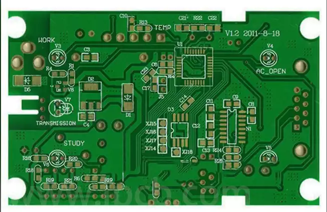
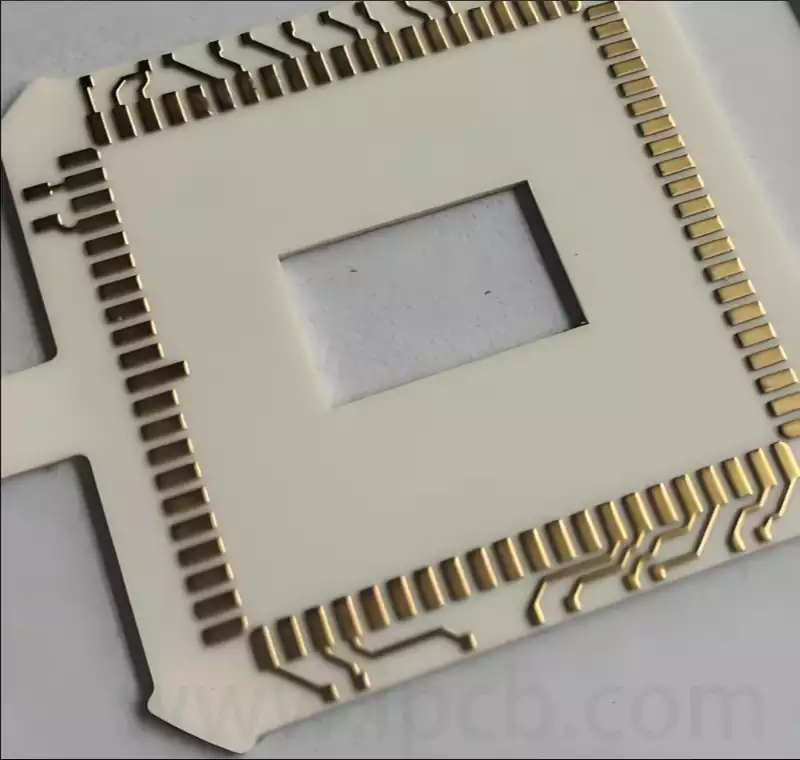
QFP Components: Use “Continuous Solder Mask Bridges” to Cover All Adjacent Pads
QFP pins are arranged in a rectangular pattern with small spacing between adjacent pins. Therefore, continuous solder mask bridges must be designed to isolate each pair of adjacent pads:
For example, in a QFP component with 0.3mm pin pitch, design a 0.1mm-wide solder mask bridge with 0.03mm spacing between each adjacent pin. This creates a “grid-like” solder mask structure, effectively preventing bridging.
BGA Components: Use Solder Mask Bridges with Caution; Prioritize Controlling Window Diameter
BGA pads are circular with small spacing between adjacent pads (e.g., 0.4mm spacing for a 0.8mm ball pitch BGA). Solder mask bridges are prone to fracture, so it is recommended:
If the pitch between adjacent pads is greater than or equal to 0.4mm: Solder mask bridges with a width of 0.1mm can be designed.
If the pitch between adjacent pads is less than 0.4mm: Prioritize resolving the issue by controlling the aperture diameter (aperture diameter = pad diameter + 0.05mm) to prevent solder mask bridge failure.
Solder mask bridges play a pivotal role in ensuring the soldering quality and performance of printed circuit boards. From the characteristics of solder mask ink, to process requirements under different copper thicknesses, to considerations for solder mask bridges on substrates and copper layers in DFM design, along with precise control of width and spacing, and adaptive designs for different component types—each aspect is interconnected and mutually influential. Only through comprehensive and in-depth mastery of these key points, coupled with strict adherence to relevant specifications and guidelines, can high-quality, highly reliable PCB boards be designed and manufactured. This ensures the stable and efficient operation of electronic devices.