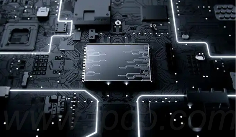
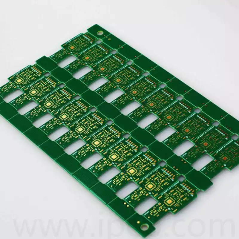
uHDI PCBs (ultra High-Density Interconnect PCB) represent a further advancement of high-density interconnect printed circuit boards (HDI PCBs). As electronic products evolve towards miniaturisation, slimness, and enhanced performance, uHDI PCBs have become a crucial foundation for next-generation electronics—particularly in smartphones, wearable devices, and high-performance computing—due to their superior routing density, smaller aperture sizes, and narrower trace widths and spacings.
uHDI PCBs incorporate numerous technical advancements over traditional HDI PCBs. Key technologies include:
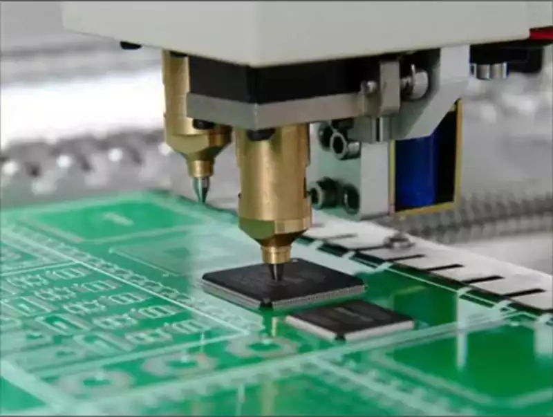
Laser drilling: Employing laser technology for hole formation enables smaller apertures and higher hole density, meeting stringent routing demands.
Micro-SAP process: The micro-subtractive additive process (mSAP) is widely adopted in uHDI PCB manufacturing, facilitating trace miniaturisation and significantly enhancing routing density.
High-precision etching technology: Within uHDI PCBs, line widths and spacings can reach as small as 10 micrometres. The exceptionally high precision requirements make etching technology a decisive factor.
Thin-layer lamination technology: uHDI PCBs typically employ multi-layer structures, necessitating lamination techniques capable of achieving extremely thin layer thicknesses while ensuring reliable electrical performance.
Future Development Trends of uHDI PCBs:
Driven by technological evolution and market demands, uHDI PCBs will evolve along these key trajectories:
Ultra-High Integration and Extreme Miniaturisation
The pervasive adoption of 5G communications, IoT ecosystems, and high-performance computing imposes stringent demands on PCB space utilisation and functional density within electronic devices. Leveraging its capability to support sub-micron line widths/spacing and compatibility with ultra-small component packages like 01005, uHDI PCB will become the core carrier in high-end consumer electronics, medical implant devices, and avionics. Future applications will extend further into cutting-edge fields such as AR/VR optical modules and 6G prototypes.
Precision Revolution and Cost Reconstruction via mSAP Process
As the mainstream uHDI manufacturing technology, modified semi-additive process (mSAP) will continually push physical boundaries. Innovations such as nanometre-level etching control and atomic layer deposition (ALD) for copper layer uniformity will enable mass production of line widths/spacings ≤5μm, while driving copper foil thickness below 1μm. This advancement will not only unlock more complex 3D stacked circuit designs but also reconfigure the cost structure of high-end PCBs through enhanced material utilisation and streamlined process steps.
Paradigm Shifts in Materials Science
Material innovation will serve as the key engine driving uHDI performance leaps. In substrate materials, low-loss (Df ≤ 0.002) and high-temperature-resistant (Tg ≥ 300°C) liquid crystal polymer (LCP) and polyimide (PI) composites will replace traditional FR-4, meeting transmission demands for millimetre-wave communications and high-speed serial signals (e.g., PCIe 6.0). Regarding copper foil, the adoption of ultra-low profile (Rz ≤ 0.5μm) carrier copper foil and nanocrystalline copper foil will substantially reduce signal attenuation. Furthermore, the integration of sustainable materials like bio-based epoxy resins will drive the industry’s transition towards closed-loop manufacturing systems.
Deep Penetration of Smart Manufacturing
Facing the precision control demands of over 200 processes in uHDI manufacturing—including laser drilling and plasma cleaning—AI-driven smart factories will become standard. Real-time process parameter optimisation via digital twin technology, sub-pixel-level defect detection in micro-holes using machine vision, and high-precision placement through adaptive robotics can elevate yield rates to over 99.98%. Concurrently, blockchain technology will establish transparent supply chain traceability systems, ensuring every uHDI PCB’s quality is traceable and accountability is verifiable.
Geopolitical Reconfiguration and Resilience-Building in Supply Chains
Amid shifting global trade dynamics, uHDI supply chains will exhibit dual characteristics: regionalised clusters coupled with strategic reserves. Enterprises will establish satellite factories in regions such as Southeast Asia and Eastern Europe, forming a ‘China + N’ production backup system. Concurrently, the local production ratio of critical raw materials (e.g., high-frequency substrates, specialised copper foil) will rise to over 40%, complemented by safety stock strategies to build resilience. Furthermore, industry alliances will drive global standardisation of the IPC-6013E universal design specification, lowering barriers to cross-regional collaboration.
Future Outlook: By 2030, uHDI PCBs will evolve into intelligent carriers integrating ‘electronic system backbone + thermal management platform + electromagnetic compatibility shielding’. Their line density will increase fivefold compared to current standards, achieving functional density exceeding 1000 I/O per square centimetre, while manufacturing costs will decrease at an annualised rate of 3%. This technology-driven transformation will not only reshape the PCB industry landscape but also serve as the physical foundation for the sixth electronic revolution.
Within PCB (printed circuit board) manufacturing, complexity primarily hinges upon the configuration of signal layers and power/ground planes required for interconnectivity. Confronted with interconnect challenges posed by next-generation semiconductors, PCB designers have effectively overcome technical bottlenecks through finer trace and spacing designs, micro-via technology, and innovative multilayer stacking strategies. When defining the complexity levels of High-Density Interconnect (HDI) or Ultra-High-Density Interconnect (UHDI) PCBs, designers must first establish clear manufacturing standards covering board outline and thickness constraints. To ensure strict compliance with predefined thickness requirements, precise targets must be set, clearly allocating the number of layers dedicated to signal transmission alongside those reserved for power distribution and grounding networks. Whilst power and ground functions may be accommodated within just two circuit layers, the specific number of signal layers requires flexible determination based on component density and interconnection complexity.
When assessing PCB design complexity, the primary consideration is the ratio of component footprint area to total board area. Should surface area constraints exist for component interfaces, multi-layer HDI manufacturing processes may be considered. To ensure successful HDI implementation, designers advancing to more complex manufacturing must fully recognise the intricacies of the process and its cost implications. Consequently, conductor routing paths must be pre-planned, with precise allocation of ‘channel spacing’ between the connection pads of vias, microvias, and component pads. The routing channel width within a semiconductor array configuration can be calculated using terminal pitch (centre-to-centre distance) and specific pad dimensions, thereby determining the maximum number of conductors per channel (i.e., conductors per channel). When channel space becomes further constrained, designers must consider internal circuit routing within the board to achieve efficient interconnections.
The industry roadmap consistently emphasises that material and process improvements remain the core drivers for enhancing product performance and manufacturing efficiency. The laminate industry is undergoing significant innovation across all materials related to encapsulation and substrate materials. For HDI applications, the selected substrate structure must possess sufficient mechanical stability to withstand the high-temperature environments encountered during PCB manufacturing and subsequent assembly processes. Although multilayer circuit board manufacturing technology is relatively mature and widely adopted, process flows and methodologies still vary among different suppliers. Faced with increasingly complex components and circuits, circuit board manufacturers must possess specialised expertise to provide solutions enabling higher-density circuit layouts. However, physical constraints frequently limit interconnect potential, primarily manifested in: ① finite PCB surface area; ② challenges posed by high component density; ③ increasing semiconductor I/O counts; ④ ultra-fine requirements for terminal spacing.
As semiconductor production complexity escalates, HDI technology emerges as an effective solution for resolving most manufacturing challenges. In circuit board design, key factors limiting interconnect routing capabilities include: ① spacing and distance between microvias or plated-through holes; ② the number of routable traces between connection pad pattern features; ③ the number of predefined signal layers.
uHDI PCBs are reshaping the future of the electronics industry through technological breakthroughs. Their miniaturisation, high performance, and sustainability will continue to drive the evolution of smart devices, establishing them as the cornerstone of the sixth electronic revolution.