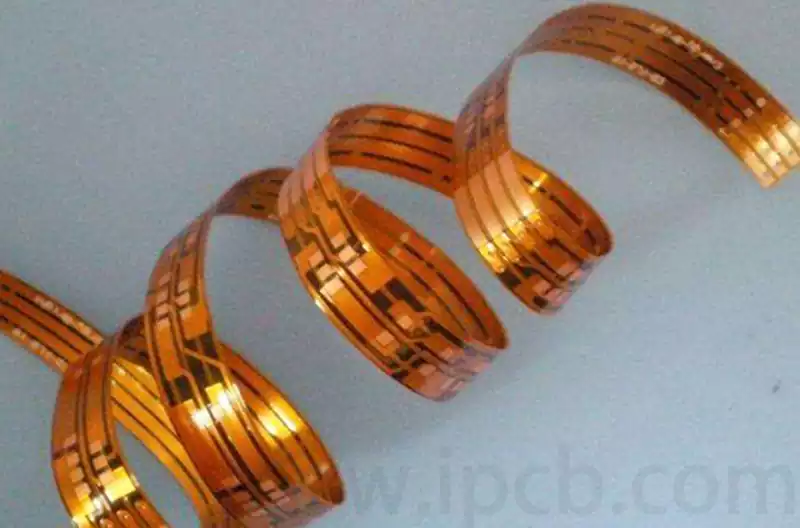
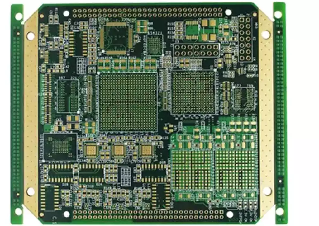
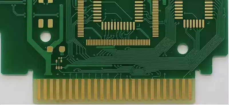
PCB Gold Fingers are a row of exposed rectangular metal contact strips along the edge of a printed circuit board (PCB). Primarily used to enable pluggable electrical connections, they serve as the critical pathway for signal and power exchange between hardware modules.
Why are gold fingers so important? The significance of PCB gold fingers is reflected in the following aspects:
Durability: Gold possesses exceptional resistance to oxidation and corrosion, meaning gold fingers remain intact even after repeated use. This resilience is crucial for maintaining the performance of electronic devices that rely on the stability of these connectors.
Conductivity: Gold is an exceptional electrical conductor, ensuring efficient signal transmission between components. This high conductivity minimizes the risk of data loss or signal attenuation, making it vital for applications requiring precise communication.
Abrasion Resistance: Gold’s hardness creates a wear-resistant surface that withstands friction from repeated insertion and removal. This durability extends the connector’s lifespan, reducing the need for frequent replacements and maintenance.
These properties make gold fingers a reliable choice for high-performance connectors. Their durability and reliability are particularly valuable in environments where devices undergo frequent assembly and disassembly. The ability to maintain stable connections under demanding conditions is precisely why they are highly favored in high-performance applications.
How Are PCB Gold Fingers Manufactured?
1.Designing the Printed Circuit Board
The first step in manufacturing gold fingers is designing the printed circuit board layout. During this phase, the placement of the fingers is determined based on the board’s intended application. Designers must ensure precise finger positioning to align with the corresponding connectors within the device.
Designers utilize precision software tools to simulate and test multiple configurations before finalizing the design. This ensures the gold fingers not only fit perfectly but also deliver optimal performance within the electronic system. Attention to detail during this phase prevents costly errors and guarantees the final product meets all necessary specifications.
2.PCB Manufacturing
Once the design is finalized, the manufacturing phase begins. This process involves PCB lamination and circuit etching. Typically, the gold finger area is left unmasked during this stage to prepare for subsequent electroplating.
Manufacturing is a critical phase where precision is paramount. Each layer of the PCB must be perfectly aligned to ensure accurate connection between the gold fingers and other components. Any deviation during manufacturing can cause misalignment, compromising the final product’s performance and reliability.
3.Gold Finger Plating Process
The plating process involves depositing a thin layer of gold onto the exposed copper contacts. This step typically comprises two sub-processes:
Nickel Plating: A nickel layer is first deposited onto the copper layer before gold plating. This nickel layer acts as a barrier, preventing copper diffusion into the gold layer and ensuring the durability of the gold-plated surface.
Gold Plating: After nickel formation, gold is deposited onto the contacts via electroplating. Gold layer thickness varies by application, typically ranging from 1.27 to 3.81 microns.
Electroplating requires strict control to ensure uniformity and compliance with quality standards. Gold layer thickness is critical, directly impacting contact durability and conductivity. Manufacturers typically conduct multiple tests at this stage to verify the plating meets all specified criteria.
4.Quality Control and Testing
After gold plating, PCBs undergo rigorous testing to ensure gold fingers meet required specifications for thickness, adhesion, and conductivity. Quality control is essential for guaranteeing the reliability and performance of gold fingers in their intended applications.
The testing process includes multiple inspections and evaluations, covering visual checks, adhesion tests, and conductivity assessments. These tests help identify defects or anomalies that could affect gold finger performance.
Ensuring high-quality standards at this stage is vital for maintaining the reputation and reliability of the final product.
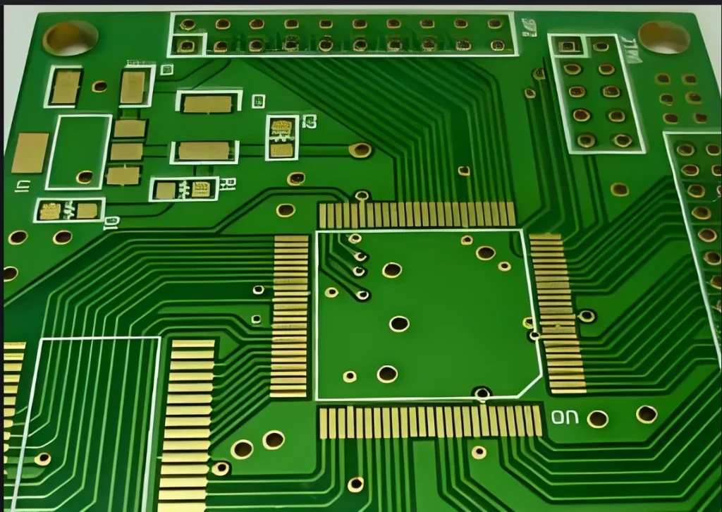
Applications of PCB Gold Fingers
Expansion Cards: Such as graphics cards, sound cards, and network cards, used to connect to the motherboard. These cards rely on gold fingers for seamless data transfer and power supply.
Connector Interfaces: Used in various electronic devices to facilitate component upgrades or replacements. Gold fingers ensure rapid, reliable connections, minimizing maintenance downtime.
Modular Electronic Devices: Suitable for equipment requiring frequent reconfiguration or component swaps. In such applications, the durability and reliability of gold fingers are vital for maintaining system integrity.
The versatility of pcb gold fingers makes them indispensable components in modern electronics. Their ability to provide reliable connections across diverse applications underscores their core value in electronic device design and functionality.
With superior durability and conductivity, pcb gold fingers play a vital role in contemporary electronic devices. Through precise design and rigorous manufacturing processes, they ensure stable and reliable electrical connections between components, making them essential key components for high-performance applications.