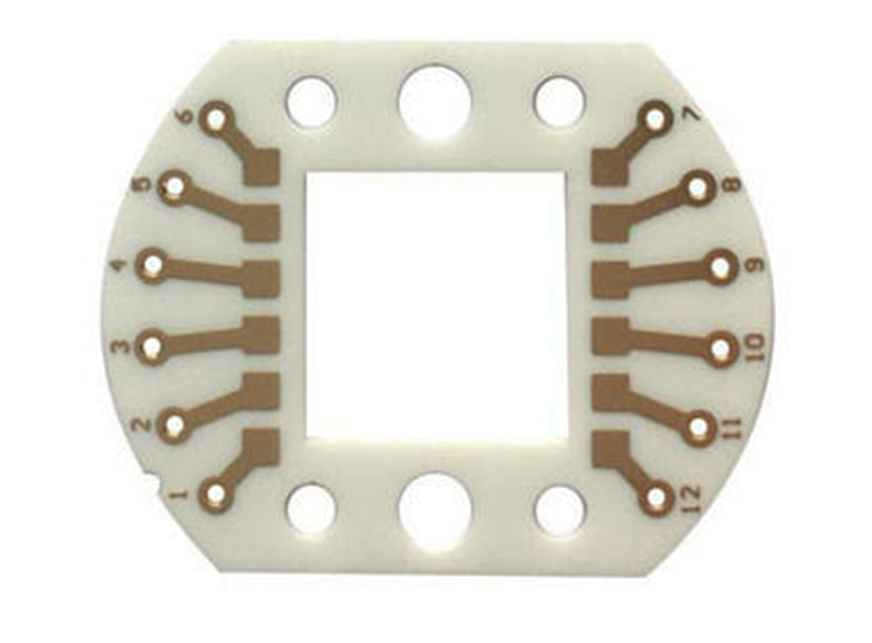
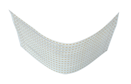
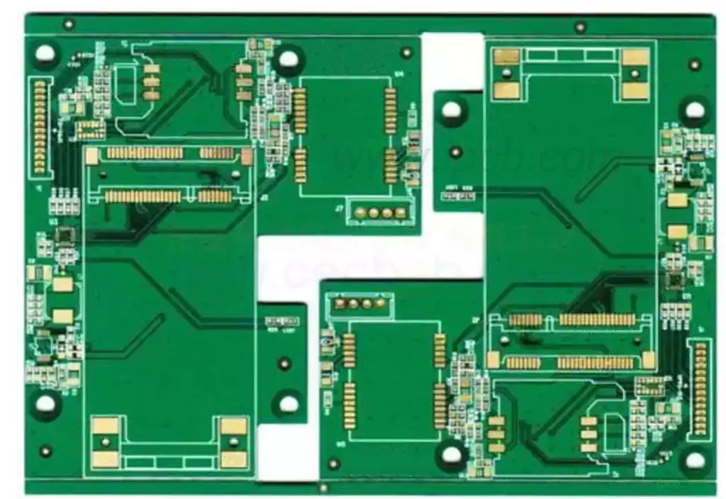
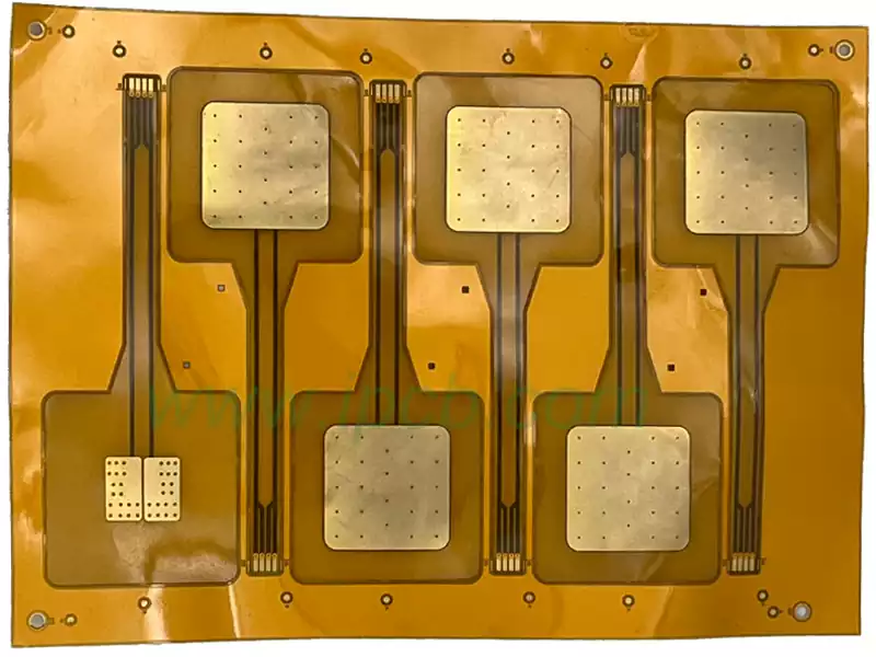
With the continuous advancement of power electronics and high-reliability electronic systems, ceramic PCBs have gained widespread application in power modules, automotive electronics, and industrial control domains due to their superior thermal conductivity, electrical stability, and environmental adaptability. However, compared to conventional FR-4 PCBs, ceramic PCBs present distinct technical constraints in routing design. Persisting with organic board routing approaches often fails to fully leverage the advantages of ceramic substrates and may even introduce new reliability risks. Consequently, achieving effective routing on ceramic PCBs necessitates systematic design considerations across multiple dimensions, including material properties, structural configurations, and electrothermal coordination.
1.Current Density and Current Carrying Capacity as Routing Starting Points
Ceramic PCBs are predominantly employed in high-power or high-current applications, where the foremost principle of routing design is to satisfy current-carrying capacity requirements. Compared to conventional PCBs, ceramic substrates typically incorporate thick copper layers, necessitating the evaluation of trace width and copper thickness based on current density considerations.
In practical design, prioritise wide and short trace configurations to avoid the localised current concentration and additional resistive heating associated with narrow, elongated traces. Simultaneously, leverage the advantages of thick copper by increasing trace width rather than adding layers to reduce resistance and temperature rise, thereby establishing the routing itself as a stable conduit for current and heat transfer.
2.Integrate thermal paths into routing planning
Routing on ceramic PCBs must not only consider electrical connections but also be synergistically designed with thermal paths. Beneath power components and in high-heat zones, avoid intricate, narrow, or sharply angled trace configurations that impede lateral heat diffusion within copper layers.
A sound approach involves designing high-current main loops as continuous, large copper areas. These serve dual functions: current conveyance alongside thermal massing and heat dispersion. Trace layouts should align with heat flow directions, minimising abrupt thermal resistance changes to maintain uniform overall temperature distribution.

3.Minimise Unnecessary Via Holes and Layer Transitions
Unlike multilayer FR-4 PCBs, via holes and interlayer interconnections in ceramic PCBs incur higher costs while introducing additional thermal resistance and stress concentration. Design efforts should prioritise reducing unnecessary layer jumps and via quantities.
For critical power circuits, single-layer or minimal-layer through-hole routing is recommended to ensure current and heat travel along the shortest path. Where vias are unavoidable, carefully control aperture size and copper fill quality to prevent current bottlenecks or potential reliability hazards.
4.Control trace width variations and corner transitions
On ceramic PCBs, abrupt trace width changes or sharp-angled turns not only cause uneven current distribution but may also create stress concentration points under thermal cycling. This issue is particularly pronounced in thick copper structures.
Therefore, routing should maintain continuous trace width transitions wherever possible, employing curved or 45° corners instead of right angles to facilitate smoother current and heat flow transitions. This design approach helps mitigate local hotspot risks and enhances the long-term reliability of metallised layers.
5.Balancing High-Frequency and High-Voltage Routing Requirements
Certain ceramic PCB applications involve systems handling both high power and high-frequency or high-voltage signals simultaneously. In such cases, routing design must strike a balance between current-carrying capacity and electrical performance.
For high-frequency signal traces, strict control of impedance continuity is essential. Reference copper planes should be strategically planned and positioned away from high-current routing areas to minimise electromagnetic interference. High-voltage traces, meanwhile, must fully leverage the ceramic substrate’s superior voltage resistance. Adequate creepage distances and electrical clearances must be established to ensure long-term operational safety.
6.Maximising the Structural Stability of Ceramic PCBs
Ceramic substrates offer high rigidity and low thermal expansion, reducing concerns about mechanical deformation during routing design. However, this does not mean stress issues can be ignored. Thick copper routing areas should be distributed reasonably, avoiding large-area copper concentration in localised zones that could cause localised thermal stress accumulation.
Through symmetrical routing, uniform copper distribution, and rational functional zoning, the stability of ceramic PCBs can be harnessed while further enhancing overall structural and routing reliability.
Effective routing on ceramic PCBs fundamentally requires moving beyond the design inertia of traditional FR-4 PCBs, adopting a systematic approach centred on high current-carrying capacity, thermal diffusion synergy, and structural reliability. By employing wide, short traces, minimising layer transitions, optimising corner configurations, and implementing integrated electrical-thermal layouts, routing not only fulfils electrical connectivity requirements but also becomes a critical component in enhancing thermal performance and system reliability. This material-property-driven routing philosophy is precisely what enables ceramic PCBs to deliver their advantages in high-power, high-reliability applications.


