Solder balls are discrete particles of molten solder that form during the reflow soldering process when the molten solder fails to wet the component leads or PCB pads properly, and subsequently splatters, separates and cools under the influence of external factors. The core mechanism behind their formation can be summarised as ‘uncontrolled solder’ – whether due to abnormal solder properties or deviations in soldering parameters, these factors can prevent the solder from wetting and spreading as intended, ultimately resulting in discrete solder balls.
According to the IPC-A-610 standard: if solder balls are distributed in non-conductive areas, with a diameter of less than 0.3 mm and fewer than three in number, they may be deemed acceptable; however, if they appear in areas where the conductive spacing is less than 0.5 mm, they are highly likely to cause short circuits and are classified as major defects that must be strictly controlled. This standard provides a clear basis for classifying defect grades and establishing key control measures.
Causes of Solder Ball Formation
1.Material Factors
Solder paste is the key influencing factor; its quality and compliance with usage specifications directly determine the likelihood of solder ball formation.
Issues with the solder paste itself: Excessive flux content (>12%) or excessive flux activity, leading to violent volatilisation during heating and causing molten solder to splatter; uneven particle size distribution or an excessively high proportion of fine powder, which tends to form fine solder balls upon melting; Improper storage (not refrigerated at 0–10°C), insufficient pre-warming or stirring prior to use, leading to moisture absorption and separation of components; during reflow, the vaporisation of moisture triggers ‘solder splatter’.
PCB and component issues: Oil, dust or oxidation on pad surfaces impair wetting; oxidation of component leads or moisture absorption by the package cause internal moisture to vaporise and expand at high temperatures, disturbing the molten solder and causing splatter.
2.Process Factors
The reflow profile and solder paste printing accuracy are critical factors in controlling solder balls.
Inappropriate reflow profile: Excessively rapid heating in the preheat zone (>2°C/s) causes rapid volatilisation of the flux; the resulting gases break through the molten solder, causing splatter; If the preheat temperature is too low or the dwell time insufficient, the flux is not fully activated; upon entering the high-temperature zone, residual solvents boil violently; if the peak temperature is too high (>245°C) or the dwell time too long, the solder melts excessively and becomes more fluid, making it prone to overflowing the pads.
Solder paste printing anomalies: Inaccurate alignment between the stencil and the PCB, or excessive separation speed, causing the solder paste to be stretched into filamentous residues that contract into solder balls after reflow; stencil apertures that are too large or too thick, or insufficient squeegee pressure, leading to excess solder paste and overflow; inadequate cleaning of the stencil underside, resulting in residual solder paste contaminating the PCB surface.
Excessive placement pressure: This forces solder paste beneath the component into the solder mask, preventing this portion of the solder from participating in normal soldering; upon cooling, it forms solder balls.
3.Design Factors
The design of the PCB and stencil determines the distribution and flow behaviour of the solder; improper design increases the risk at the source.
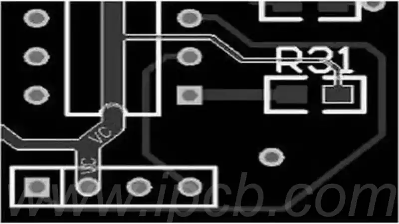
PCB design defects: Absence of solder mask around pad edges or excessively large apertures, allowing solder to spread into non-pad areas; lead-to-pad spacing >0.2 mm, causing excess solder to contract into solder balls under surface tension; poor surface flatness, resulting in uneven solder paste printing.
Inappropriate stencil design: apertures larger than the pads; for example, apertures for surface-mount components exceeding 70% of the pad width, resulting in excess solder paste; failure to use anti-balling apertures (such as inverted trapezoidal or concave dovetail shapes), increasing the likelihood of solder paste overflow.
4.Environmental Factors
Control of workshop temperature and humidity is often overlooked, yet indirectly influences solder ball formation.
Excessive humidity (>60% RH): Accelerates moisture absorption by the solder paste and the PCB, increasing the likelihood of ‘solder splatter’.
Significant temperature fluctuations: Affect the viscosity and flow properties of the solder paste, reducing printing accuracy.
Excessive dwell time after printing (>8 hours): The solder paste absorbs moisture and solvents evaporate, causing performance abnormalities and making it prone to solder ball formation.
Solder Ball Control Measures
1.Material Control: Establish a comprehensive system covering the entire process from “selection—storage—use”
Selection: Give priority to lead-free solder paste with uniform particle size (e.g. Type 4, 20–38 μm), moderate flux content (10% ± 1%), and good oxidation resistance (e.g. Sn96.5Ag3.0Cu0.5); Strictly inspect the cleanliness and oxidation status of PCB and component surfaces upon receipt; bake moisture-sensitive components (QFP, BGA, etc.) according to their humidity sensitivity levels.
Storage and Use: Store at 0–10°C; allow to warm up for 4 hours before use and stir for 5–10 minutes; use as soon as possible after opening, and reseal and refrigerate any unused portion promptly; the use of expired or deteriorated solder paste is strictly prohibited.
2.Process Optimisation: Focusing on the two core stages of printing and reflow soldering
Solder paste printing: Optimise stencil alignment accuracy; adjust separation speed to 0.5–1 mm/s; for surface-mount components, set aperture width to 60–70% of pad width and length to 80–90%, and use anti-balling apertures; Clean the underside of the stencil and the squeegee regularly; use an SPI (solder paste inspector) to perform 100% inspection of print quality.
Reflow Soldering Profile: Adopt a strategy of “gradual heating, thorough preheating, and precise temperature control” — preheating zone 120–150°C, heating rate ≤1.5°C/s, hold for 60–90 seconds; Peak temperature 235–240°C, held for 10–15 seconds; cool down gradually in the cooling zone. Calibrate oven temperatures regularly to prevent localised overheating.
Placement: Control placement pressure (small components <3 N) to ensure placement accuracy and prevent solder paste extrusion.
3.Design Optimisation: Reducing Solder Ball Risks at Source
PCB Design: Pin-to-pad spacing ≤ 0.15 mm; apply a solder mask with a width of ≥ 0.1 mm at pad edges; optimise surface flatness; design thermal isolation pads for high-density pin components (QFP, BGA).
Stencil Design: Ensure strict alignment with PCB pad dimensions; use inverted trapezoidal or concave dovetail openings for surface-mount components prone to solder balling; control stencil thickness to 0.1–0.13 mm; liaise with the production department during the design phase to prevent discrepancies between design and process.
4.Environmental Control: Standardised Production Environment
Maintain a temperature of 23±5°C and humidity of 40–60% RH; install real-time monitoring equipment and make prompt adjustments in the event of anomalies.
Complete component placement and reflow within 4 hours of solder paste printing; clean the workshop regularly to minimise contamination from dust and impurities.
5.Inspection and Rework: Closed-Loop Control
Inspection: SPI inspection after printing, followed by AOI (Automated Optical Inspection) after reflow to rapidly identify the position, size and quantity of solder balls, and promptly intercept defective products.
Rework: Solder balls within acceptable limits require no further action; for non-conforming solder balls in conductive areas, clean using an anti-static brush with isopropyl alcohol; stubborn residues may be removed by heating with a heat gun and then picking up with tweezers. Post-rework electrical testing ensures there are no short-circuit risks, thereby reducing the scrap rate.
Preventing solder balls requires a multi-faceted, coordinated approach involving materials, processes, design and the environment in order to achieve stable and reliable soldering quality.