Multilayer microwave circuit boards are specialised printed circuit boards designed for high-frequency applications. Through a composite structure of multiple layers of insulating substrate and conductive copper foil, they enable the efficient transmission of electromagnetic waves and functional integration. Their core lies in the use of microwave transmission structures such as microstrip lines and striplines to achieve parallel signal processing with low loss and high stability; they are widely used in fields such as communications, radar and aerospace.
Core Operating Principles of Multilayer Microwave Circuit Boards
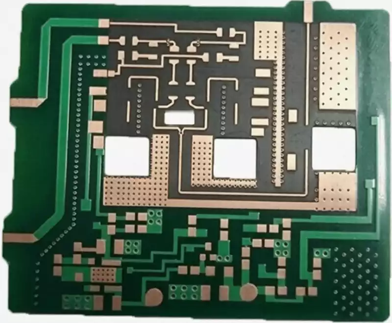
Multilayer microwave circuit boards are constructed by alternately laminating multiple layers of insulating substrate and conductive copper foil. Electrical isolation between circuit layers is achieved through the insulating layers, whilst electromagnetic signal transmission is facilitated by the conductive copper foil layers. Their core operating logic is based on microwave transmission line theory. Through specialised microwave transmission structures integrated into the board, such as microstrip lines and striplines, they achieve the precise transmission, coupling and distribution of electromagnetic waves.
Compared to standard circuit boards, multilayer microwave circuit boards overcome the layout limitations of single-layer circuits. They enable the separation of multiple signal paths and the synchronous parallel transmission of multiple channels, allowing for the high integration of various microwave functional circuits and significantly reducing equipment size. Furthermore, their excellent high-frequency adaptability, low loss and low signal distortion characteristics meet the requirements for high-speed, high-frequency and highly stable signal transmission, making them widely applicable in high-end fields such as high-speed communications, radar detection, satellite communications, medical imaging and military electronics.
Basic Structural Composition of Multilayer Microwave Circuit Boards
Multilayer microwave circuit boards consist of a multi-layer composite integrated structure, with each layer having a clearly defined role and complementary functions. The core components are divided into four categories, which collectively ensure the stable transmission of microwave signals:
1.Substrate Layer: Serving as the fundamental supporting structure of the circuit board, it primarily utilises materials with excellent high-frequency performance, such as glass fibre, ceramic and polyimide. It possesses high strength, low dielectric loss, high-temperature resistance and resistance to deformation, providing stable support for the conductive and insulating layers.
2.Conductive foil layer: With high-purity copper foil as the core material, this serves as the primary medium for the transmission of electromagnetic waves and high-frequency signals. Through etching, it forms various microwave transmission lines, functional circuits and pads, enabling the conduction of electrical power and electromagnetic signals.
3.Insulation Layer: Primarily utilising high-frequency, low-loss insulating materials such as PTFE, FR-4 and ceramics, this layer is positioned between the conductive layers. Its primary function is to provide electrical isolation between layers and channels, eliminating crosstalk and leakage, thereby ensuring the independence and stability of signal transmission.
Attenuation and Coupling Layer: A functional layer specific to microwave circuits, it enables the conversion, coupling and attenuation control of electromagnetic wave energy. At the same time, it effectively blocks signal feedback, suppresses self-oscillation interference, and enhances the circuit’s overall immunity to interference and operational stability.
Core Application Areas of Multilayer Microwave Circuit Boards
Thanks to their core advantages—strong high-frequency adaptability, high data transmission rates, low signal loss, high integration, and excellent stability—multilayer microwave circuit boards have become essential components in high-end electronic and information technology equipment. Their applications span a wide range of sectors, including civil communications, industrial detection, defence and aerospace, and medical equipment.
In the field of high-frequency microwave communications, these circuit boards support high-speed, high-capacity data transmission and multi-site synchronous communication. Thanks to their efficient and stable transmission characteristics, they ensure the normal operation of equipment such as 5G/6G communication systems and microwave relay systems.
In the field of radar detection, radar systems require the real-time and precise acquisition of data such as target distance, velocity, bearing, environmental meteorological conditions and signal strength. Through multi-channel parallel transmission technology, multilayer microwave PCBs significantly reduce signal transmission latency and waveform distortion, thereby markedly enhancing radar detection accuracy and response speed. Furthermore, they are widely used in scenarios with extremely high demands for signal quality, stability and integration, such as satellite communications, aerospace equipment, high-precision medical imaging and military measurement and control.
Core Technologies for Grounding in Multilayer Microwave PCBs
Core Objectives of Grounding
1.Establishing a low-impedance, continuous signal return path: High-frequency currents preferentially return via the path with the lowest inductance; a complete, high-quality ground plane is essential for achieving low-loss return paths.
2.Ensuring reference plane integrity: Providing a tightly coupled, complete ground reference plane for microwave transmission structures such as microstrip lines and striplines, thereby stabilising the characteristic impedance of transmission lines and preventing issues such as signal reflection and increased loss caused by sudden impedance changes.
3.Achieve electromagnetic shielding and channel isolation: Effectively isolate electromagnetic crosstalk between digital and analogue circuits, RF and IF modules, and channels operating in different frequency bands, thereby preventing mutual interference between modules.
4.Suppress noise and resonance interference: Minimise the generation of ground loops and ground bounce noise, and reduce issues related to parasitic resonance and noise coupling in circuits.
5.Enhance heat dissipation: A large, continuous ground plane offers excellent thermal conductivity and serves as the primary heat dissipation pathway for high-frequency, high-power microwave devices.
Key Grounding Strategies and Implementation Methods
1.Scientific Layering to Ensure Ground Plane Integrity
Layered design forms the foundation of microwave PCB grounding optimisation. The core principle is to configure dedicated, continuous ground planes, ensuring that signal layers are positioned immediately adjacent to the ground plane. Priority should be given to establishing dedicated, continuous ground planes made of solid copper for microwave circuits. Critical microwave signal lines and striplines must be sandwiched between two ground planes, and a complete reference plane must be provided beneath microstrip lines; signal lines must not be routed across segmented ground planes.
For circuit boards of different layer counts, standardised optimal layering schemes should be adopted: for four-layer boards, the preferred structure is “top-layer signal/ground – ground plane – power layer – bottom-layer signal/ground”; For six-layer boards, the preferred structure is “top-layer signal – ground plane – inner-layer stripline signal – power layer – ground plane – bottom-layer signal”, sandwiching the core microwave signals between two ground planes to achieve optimal shielding and impedance control; for eight-layer and higher-order boards, additional dedicated ground planes may be added to physically segregate sensitive circuit areas with different functions or operating frequencies.
2.Dense Grounding Vias to Establish a Three-Dimensional Low-Impedance Ground Network
Grounding vias (via stitching) are the core method for connecting ground planes across layers and reducing ground inductance. Ground vias must be densely placed at critical locations, such as around component ground pads, on both sides of microwave transmission lines, at the edges of ground planes, at the junctions of functional modules, and in areas where shielded enclosures are installed. Viaspacing must be strictly matched to the operating frequency; as a general rule, it should be kept within 1/10 of the wavelength at the highest operating frequency (e.g., spacing must be less than 3 mm for the 10 GHz band), whilst high-precision applications may be routed to a λ/20 standard.
Concurrently, low-inductance via designs should be adopted, utilising small-diameter vias of 8–12 mils to ensure complete and uniform copper plating on the via walls. For ground pads on the underside of chips, through-hole-in-pad (THIP) technology may be employed to minimise ground paths and reduce ground inductance. The issue of floating copper planes must be avoided throughout the design; all ground copper layers on both outer and inner layers must be reliably connected to the main ground plane via vias to eliminate floating ground islands.
3.Optimising Component Grounding and RF Port Grounding
For core components such as microwave chips, transistors and ground capacitors, large-area ground pads must be designed and directly connected to the inner-layer main ground plane via via arrays, thereby significantly reducing component ground inductance. For RF connectors such as SMA and SSMA, the housing ground pins must utilise a multi-via array grounding scheme to achieve low-impedance, all-round grounding. High-power microwave devices require dedicated thermal grounding pads and dense via arrays to balance grounding stability with thermal dissipation efficiency.
4.Strictly control ground plane segmentation to eliminate signal crosstalk
The ground plane in the core microwave operating area must be kept as complete and continuous as possible, minimising slotting and segmentation operations. Ground plane segmentation may only be undertaken with caution at the junctions of different functional modules or in special scenarios requiring high isolation; it is strictly prohibited for microwave signal lines to be routed across segmentation slots, ensuring that the reference plane for signal transmission paths remains unbroken.
If ground plane segmentation is unavoidable, only low-frequency and DC control signals are permitted to cross the segmented areas. Signal bridging may be achieved by reserving narrow channels on the power supply layer or an independent signal layer, whilst strictly avoiding microwave signals crossing between zones. Furthermore, the independent ground planes resulting from segmentation must be interconnected at multiple points—such as signal bridging locations and module edges—via vias or high-frequency bypass capacitors to eliminate ground potential differences and suppress high-frequency interference.
5.Standardise Top-Layer Grounding to Enhance Shielding Protection
On the top layer of the circuit board, all areas except those occupied by signal lines must be fully covered with copper for grounding. These areas must be connected to the main ground plane via densely spaced stitched vias. This approach not only provides electromagnetic shielding and reduces signal radiation leakage but also increases the number of ground paths and lowers ground impedance.
During ground plane routing, spacing must be strictly controlled to ensure that the distance between the edge of the copper plane and microwave signal lines is no less than three times the line width, thereby preventing parasitic capacitance from affecting the characteristic impedance of the lines and increasing transmission loss. Solid copper ground planes should be prioritised in microwave and high-frequency areas, whilst mesh ground planes may be used in low-frequency digital areas as appropriate to balance thermal dissipation and electrical performance.
6.Partitioned shielding and isolation to suppress crosstalk between modules
For modules that are sensitive to mutual interference—such as power amplifiers, low-noise amplifiers, oscillators and channels operating in different frequency bands—a dual isolation scheme is employed. Firstly, a via shielding wall is constructed by densely arranging multiple rows of ground vias along the module boundaries to form a closed electromagnetic barrier, thereby blocking electromagnetic crosstalk between modules;
Secondly, for core modules requiring ultra-high precision and stability, a metal shielded cavity structure is employed. The copper layer on the surface of the shielded cavity installation area must be complete and free of gaps, and all inner ground planes are connected via a dense array of vias to achieve 360° low-impedance ground shielding.
7.Simulation and experimental verification to ensure grounding performance meets standards
During the design phase, professional electromagnetic simulation tools such as HFSS, CST and ADS Momentum can be used to perform 3D electromagnetic field simulations of the grounding structure, via arrays and shielding isolation effects, verifying key metrics such as S-parameters, channel isolation and circuit resonance characteristics, and optimising grounding defects in advance. Concurrently, power integrity and signal integrity simulations are conducted to assess the impact of ground bounce noise and ground loops on the circuit. Following the completion of board fabrication, parameters such as signal loss, standing wave ratio and isolation are measured using a vector network analyser to comprehensively verify the reliability of the grounding design.
Thanks to their excellent high-frequency compatibility, high integration capabilities and stable signal transmission performance, multilayer microwave circuit boards have become an indispensable piece of basic hardware in modern high-end electronic information equipment. As communication frequencies evolve towards millimetre-wave and terahertz bands, the demands on the integration, stability and grounding precision of multilayer microwave circuit boards will increase further, which will in turn continue to drive innovation and breakthroughs in related design methods and manufacturing processes.