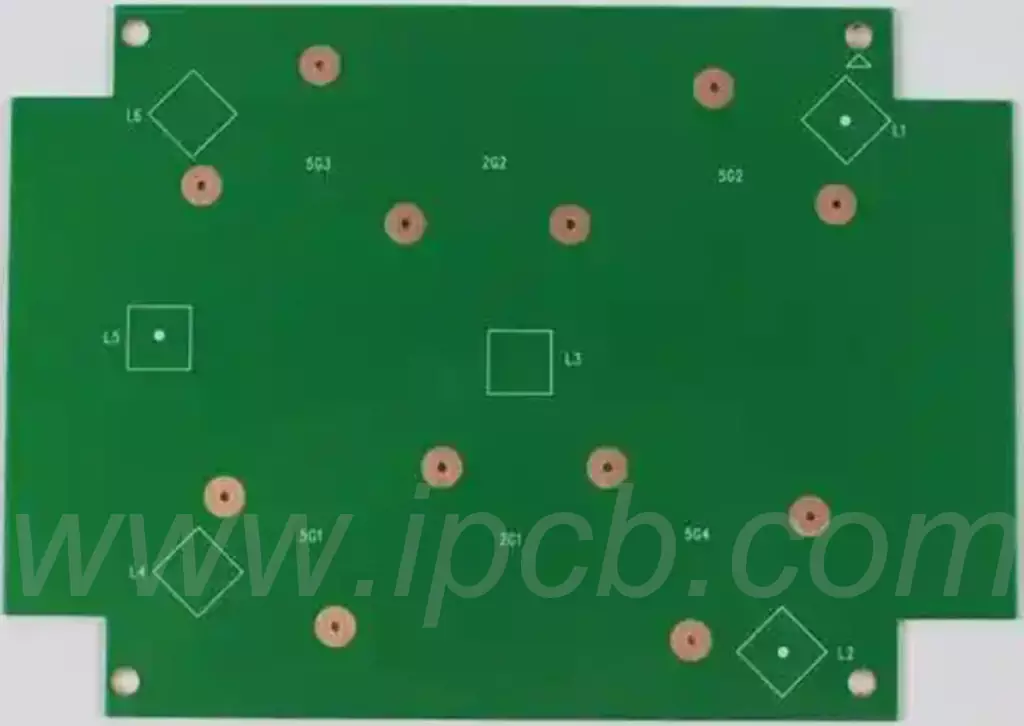
Unveiling the Microscopic Topology of Thick-Film Ceramic Substrates
Unlike traditional circuit boards manufactured by laminating copper foil, the creation of thick film circuit boards is a magical transformation of inorganic materials at near-thousand-degree Celsius temperatures. Conductive, insulating, or resistive pastes are deposited onto a ceramic substrate using precision screen printing, followed by extremely demanding high-temperature sintering, microscopically reconstructing a functional film layer typically 10 to 25 micrometers thick.
The lattice rigidity and limiting thermal conductivity of the ceramic substrate are the physical framework upon which thick-film circuits rely. These are special inorganic ceramic sheets with extremely high hardness and chemical stability. Based on different power densities and cost profiles, the supply chain is mainly divided into three core crystal camps: high-purity alumina (Al2O3, typically 96% to 99.6%): It is the absolute uncrowned king of the thick-film industry. It possesses exceptional mechanical rigidity, high dielectric strength, and remarkable physical inertness even under 850°C sintering conditions.
Its thermal conductivity is approximately 25 W/m·K, which, while not outstanding, is still hundreds of times higher than that of ordinary FR4 resin, easily surpassing the heat dissipation limits of conventional consumer electronics. Aluminum nitride (AlN): In laser pump sources or high-power IGBT modules where extreme heat flux density is required, the thermal resistance of alumina becomes insufficient. Aluminum nitride, with its exceptional intrinsic thermal conductivity ranging from 170 W/m·K to 230, acts as a “heat bomber” in the microscopic space. Meanwhile, its linear thermal expansion coefficient (4.5 ppmC) is extremely close to that of third-generation semiconductor silicon and silicon carbide (SiC) wafers (approximately 3.7 to 4.0 ppmC), inherently preventing interlayer shear force delamination cracking under extreme cold and heat cycles.
Beryllium oxide (BeO): Possesses unparalleled thermal conductivity exceeding 250 W/mK, but due to the severe biotoxicity of its micropowder, it currently only holds a narrow market share in aerospace high-power traveling wave tubes and certain extreme radar RF front-ends.
The microscopic anchoring and three-dimensional metallurgical locking mechanism of the glass phase in the slurry: Before sintering, thick film slurries are viscous multiphase fluids composed of micron-sized metal powders, inorganic glass powders, and organic carriers (such as terpineol and ethyl cellulose). After screen printing precisely places the trace pattern onto the ceramic surface, the motherboard is pushed into a depth of up to 850… In a multi-zone mesh belt sintering furnace (C), the organic fluid carrier is completely vaporized and burned off in the early temperature zones, leaving behind a tightly packed layer of dry metal and glass powder.
When the temperature reaches its peak, the inorganic glass powder (usually borosilicate glass) within the slurry undergoes physical melting, degenerating into a flowing liquid phase. This molten glass layer rapidly penetrates downwards due to capillary action, aggressively wetting the rough, uneven microcrystalline boundaries of the ceramic substrate. Simultaneously, the metal particles within the slurry (such as pure silver, silver-palladium alloys, gold, and platinum) also begin solid-state diffusion and sintering. Necks grow and interconnect to form dense, three-dimensional, continuous conductive metal frameworks. As the furnace temperature slowly decreases, the molten glass that has penetrated the ceramic surface solidifies, forming countless microscopic “inorganic chemical barbs” that firmly grip the ceramic lattice.
On top, this glass phase is deeply intertwined with the sintered metal mesh. This unique inorganic-metal metallurgical locking structure gives the thick film traces exceptional adhesion strength, enabling them to withstand prolonged high-temperature oxidation bombardment without physical delamination.
Cermet Transitions in Resistor Paste and Laser Precision Resistor Repair
On a high-specification thick film circuit board, the most astonishing optical and electrical feature is its ability to directly “print” hundreds or thousands of high-precision functional resistors onto the ceramic surface. These resistor components are not soldered-on patches, but rather cermet isomers grown in situ through paste sintering. Resistors.
The Microscopic Code of Resistance Width: Percolation Theory of Ruthenium Dioxide (RuO2) To simultaneously fabricate current-limiting resistors of a few ohms and high-voltage sampling resistors of several megaohms on a single substrate, thick-film material scientists must precisely tune the distribution of microscopic conductive particles within the resistive paste. Currently, mainstream thick-film resistive pastes comprehensively utilize noble metal oxides such as ruthenium dioxide (RuO2) or bismuth ruthenate (Bi2Ru2O7) as the conductive phase, doping them into a large amount of insulating glass powder matrix. In microscopic low-resistivity pastes, ruthenium dioxide particles constitute a very high volume, colliding closely with each other in space, building countless dense, highly resistive pure metallic conductive pathways. In high-resistivity pastes, however, ruthenium dioxide particles are diluted to a large proportion.
At this point, the conductivity mechanism of the resistor enters the extremely mysterious percolation and tunneling effects in electromagnetism. In the field of (Effect) resistors, conductive particles no longer make direct physical contact but are separated by layers of nanoscale thin glass insulating barriers. Charges must rely on the tunneling effect in quantum mechanics to “jump through” the barrier. This structure endows thick-film resistors with extremely strong resistance to high-voltage surges and electrical pulses. Because its volume is much larger than the thin film layer of a conventional chip resistor, a sudden influx of thousands of volts of high-voltage charge can be uniformly dissipated and buffered within the vast three-dimensional glass-ceramic matrix, preventing localized overload burnout. However, the initial resistance accuracy of this multiphase hybrid structure after sintering is often extremely poor, with errors typically between ±10% and 20%, making it unsuitable for direct delivery to precision medical instruments or high-voltage battery management systems.
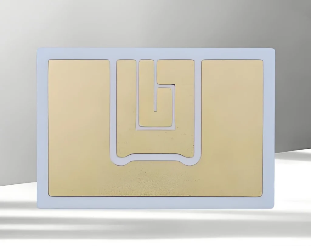
Laser Trimming, with its optical evaporation and microscopic resolution control, aims to forcibly compress the resistance error of printed resistors from 20% to a terrifying 0.1% or even 0.01%. For aerospace-grade precision, thick-film mainboards must be fed into a high-energy neodymium Jacobian (Nd:YAG) infrared or green laser resistance repair machine production line. Inside the repair chamber, a high-frequency probe is instantly pressed against the two end electrodes of the resistor, monitoring its resistance change in real time. Simultaneously, a laser beam, focused with high-magnification optical resolution, is vertically bombarded on the resistor surface at a pulse velocity of several kilohertz. The high energy density of the laser beam causes the ruthenium dioxide and glass mixture at the impact point to undergo instantaneous sublimation and thermochemical evaporation within one microsecond, smoothly cutting an “L” or “U” shaped groove on the resistor sheet. A physical cut, either “serpentine” or “snake-shaped,” is created.
As the laser source moves forward, the effective conductive cross-sectional area of the resistor is gradually reduced, causing the resistance to rise linearly and steadily. The laser is switched off within a nanosecond at the exact moment the resistance value fed back by the probe falls within the target tolerance dead zone set by the main control chip. This process not only eliminates the welding thermal stress on the components from external mechanical forces but also utilizes laser evaporation technology to precisely control the resistance and temperature coefficient (TCR). The PM50 (ppmC) level was adjusted to a near-perfect physical equilibrium, creating an absolutely precise microscopic barrier for high-voltage power measurement and control.
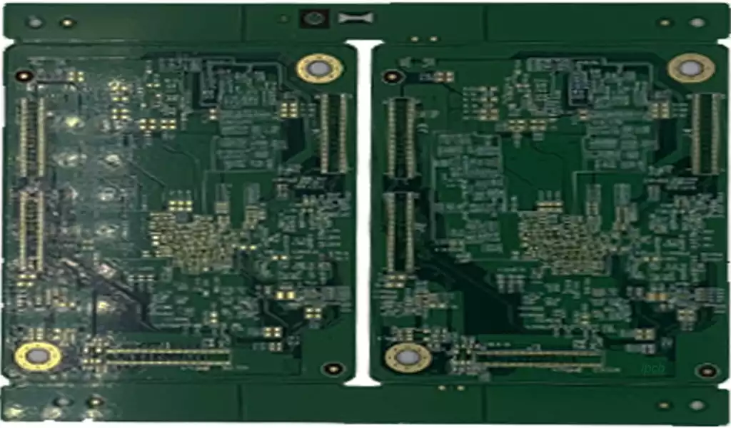
Multilayer Wiring, Electromagnetic Silver Migration, and Thermoelectric Separation
As thick film circuit boards move towards more complex microwave radar components or hundreds-volt new energy vehicle OBC control motherboards, multilayer printed wiring and the electrochemical migration of metal atoms become the most brutal nightmare in the entire system reliability testing phase. 3.1 Repeated Sintering and Micropore Encirclement of Multilayer Thick Films To achieve complex cross-wiring on ceramic sheets, similar to traditional multilayer PCBs, thick film processes must employ an alternating printing-sintering method.
After the first layer of metal conductors is sintered, engineers must screen-print a special low-dielectric-constant (Low-K) crystalline glass insulating dielectric paste across the entire board. At the vertical projection points where electrical conduction between upper and lower layers is required, a stencil is used to deliberately leave a diameter of 150 mm. The dielectric layer consists of micro-perforations (visas) of approximately one micrometer in diameter. This dielectric layer undergoes a secondary sintering and curing process at 850°C. At this point, the dielectric layer faces a critical physical defect—microscopic pores and pinholes.
Trace bubbles left from the volatilization of organic matter, if not perfectly filled by their own fluid surface tension during the glass melting stage, will leave a microscopic hollow channel running straight to the bottom within the several-micrometer-thick insulating layer. When a second layer of metal wire is subsequently printed on the outer layer and the vias are filled, followed by a third or even fourth round of repeated high-temperature sintering, the molten metal from the outer layer will undergo physical capillary penetration downwards along these invisible dielectric pinholes, causing in-situ, invisible interlayer flashover short circuits between the independent signal lines of the upper and lower layers within the furnace.
To seal this physical curse of pinholes, advanced thick-film processes must introduce double printing and double sintering (Double Printing & Double Sintering) into the dielectric layer. The Firing strategy involves continuously printing two extremely thin layers of dielectric paste. Utilizing statistical principles, randomly generated pores and pinholes within the two layers are staggered in a vertical three-dimensional space, achieving 100% physical interleaving. This fundamentally cuts off the pathway for molten metal penetration, dramatically increasing the interlayer breakdown strength to over 50 volts per micrometer, reaching peak automotive-grade levels.
Silver migration (Silver) Electrochemical Tamping of Gold, Platinum, and Palladium: The Metallurgical Balance In the pursuit of ultimate cost-effectiveness in thick-film multilayer board designs, pure silver (Ag) paste has long been the preferred choice for high-current conductors due to its extremely low volume resistivity and affordable price. However, pure silver is an extremely aggressive “electrochemical terrorist” in harsh operating environments characterized by humidity, trace amounts of moisture, and a continuous DC electric field. Silver atoms readily ionize into free silver ions (Ag+) in the surface water film. Driven by the strong electric field of a DC voltage, these silver ions frantically migrate along the microscopic capillary gaps of the ceramic substrate towards the low-potential negative electrode. A physical migration occurs. Once it touches the negative electrode, the silver ions regain electrons and are reduced to pure metallic silver in situ, precipitating out.
This process repeats itself. Under a microscope, metallic silver uses the negative electrode as a base to grow in reverse towards the positive electrode, forming tree-like or antler-like metallic dendrites. When the tips of these dendrites finally cross a gap of tens of micrometers and physically touch the positive electrode, a violent metal short circuit is triggered, causing the entire previously absolutely insulated signal line to fail. To completely subdue the curse of silver migration, the high-end thick-film industry has fully launched a defense strategy using precious metal metallurgy. This involves precisely controlling the silver ions within the pure silver layer by weight percentage (e.g., … A 3:1 or 6:1 ratio of highly inert palladium (Pd) or platinum (Pt) metal particles is forcibly fused in, forming a robust silver-palladium/silver-platinum solid solution alloy conductive phase.
When silver atoms attempt to ionize, the tightly packed palladium atoms utilize their strong lattice barrier and electron shell attraction to lock in the ionization kinetic energy of the silver, instantly increasing the overall resistance to silver migration and solder leaching several times over. In higher-level military RF and microwave radar modules, a full-gold (Au) paste process is directly adopted. Utilizing the absolute inertness of pure gold atoms—which cannot be electrochemically oxidized under any natural environment—a physical longevity certificate for absolute reliability is issued to the entire multilayer high-frequency microwave thick-film motherboard.
Agile NPI Strategy for Ceramic Thick-Film Circuits
As global research and development of extreme hardware such as hybrid electric vehicle cabins, deep-sea high-pressure oil field exploration, and commercial aerospace microsatellite propulsion systems enters a fever pitch, thick film circuit boards… The applications of ceramic thick-film circuits are spilling over from a few traditional military-industrial zones to the broader high-end industrial manufacturing landscape. However, due to the extremely capital-intensive processes involved in high-temperature metallurgy, precision screen printing, and laser precision resistivity adjustment, ceramic thick-film circuits have long maintained a formidable barrier to entry in the supply chain.
The “high barriers” of traditional large manufacturers and the “high walls of prototyping” in hardware R&D mean that in the current microelectronics supply chain, factories possessing complete capabilities in thick-film printing, sintering, multilayer dielectric alignment, and laser resistivity adjustment are almost exclusively a few long-established, monopolistic research institutes and listed giants deeply embedded in the specialized supply chains of the military and heavy-haul railway systems. These traditional entities face the ever-changing market… Agile innovation often exhibits an extremely rigid and disconnected supply chain approach: Because thick-film processes require hours to heat up and balance temperature curves across multiple zones each time the furnace is opened, and the production cost of the stencil for screen printing and the capital tied up in special precious metal pastes (gold, platinum) are substantial, these traditionally monopolistic factories typically refuse to undertake any small-scale engineering modifications.
Their business barriers often include extremely high minimum order quantities (MOQs) or exorbitant material handling fees. If agile innovative companies or cutting-edge university labs urgently need to modify the parameters of a few power resistors for system performance prototyping, they often face lengthy business approval cycles, with delivery times ruthlessly extended to 6 to 8 weeks or more. In the life-or-death race of hardware R&D where “delivery time is life,” such prolonged cycles can easily kill a potentially disruptive innovative hardware project before it even reaches its cradle.
To break free from the time constraints of R&D prototyping and small-batch production of special microelectronic ceramic substrates, a truly aerospace-grade reliable agile thick-film R&D hub has been established by a leading process service provider through a complete set of flexible reconstruction, creating a dedicated “green reaction hub for thick-film ceramic circuits”. Manufacturers maintain a year-round stock of 96% alumina and high thermal conductivity aluminum nitride ceramic substrates. They have also implemented fully digital dynamic choreography for their fully automated screen printing machines, multi-temperature zone precision micro-adjustment mesh belt sintering furnaces, and four-axis high-precision laser trimming systems, ensuring complete backward compatibility with the prototyping and R&D stages. This results in a truly absolute zero-MOQ engineering response: whether it’s a high-density multilayer silver-palladium thick film board or an alumina board integrating precision laser trimming metal-ceramic resistors, in the early stages of NPI (New Product Introduction), even if a customer only needs 2 or 5 engineering verification samples due to extreme environment verification, the senior engineering team will instantly initiate a 1-on-1 expert-level Design for Manufacturability (DFM/DFA) process review, with absolutely no minimum consumption or quantity restrictions.