Decoding the Signal Integrity and Impedance of BGA Adapter Boards
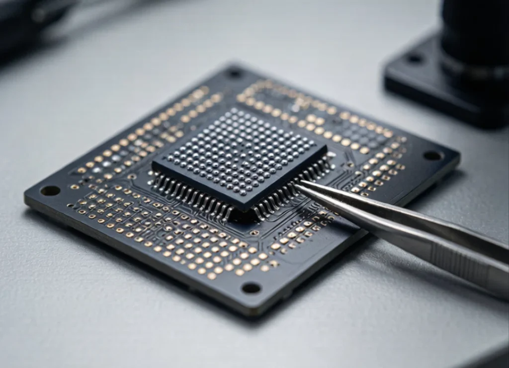
The core physical purpose of BGA adapter boards is to fan out the incredibly dense, unsolderable BGA pin matrix on the bottom in three dimensions and retopologically refactor it into a more open interface (such as standard-pitch pads, pins, or dedicated connectors for high-speed logic analyzers). However, within this three-dimensional fan-out channel transitioning from the microscopic to the macroscopic, high-frequency alternating electromagnetic waves face extremely harsh physical obstacles.
The Limiting 50-Ohm Characteristic Impedance Control and the Parasitic Black Hole of Microvias
When a high-speed signal line with a rate of tens of Gbps (such as PCIe 5.0, USB4, or high-frequency RF signals) flows through a BGA adapter board, the dielectric layer, electric field, and magnetic field surrounding the conductor collectively determine its characteristic impedance. Adapter boards are typically extremely thin. To achieve precise 50-ohm single-ended or 100-ohm differential impedance control on a board the size of a fingernail, trace width and interlayer dielectric thickness must be squeezed down to the micrometer level.
An even more terrifying electromagnetic trap lies within the vertical vias. Due to the extremely compact size of BGA pins, adapter boards must fully incorporate laser-drilled microvias and stacked vias. On a typical printed circuit board, a via is simply a conductive conduit; however, at high-frequency bandwidths of tens of gigahertz (GHz), the metal walls of each vertical via, and any incompletely milled stubs, degenerate into microscopic parasitic capacitance and inductance structures.
If the plating of the blind vias is uneven during adapter board manufacturing, or if air gaps exist within the vias, these tiny parasitic parameters can induce strong electromagnetic wave reflection impedance discontinuity in situ. When high-frequency electromagnetic waves strike a via, they cause severe reverse current, much like light striking a mirror, resulting in a completely closed eye diagram of the signal ultimately delivered to the testing instrument.
Therefore, the manufacturing process of advanced BGA adapter boards must incorporate cutting-edge 3D electromagnetic field full-wave simulation technology during the CAM computer programming stage. This involves micron-level fine modeling of the ground shielding rings surrounding the vias, forcibly limiting impedance fluctuations introduced by the vias to within the absolute automotive-grade limit of ±5%.
Physical Elimination of High-Density Proximity Effect and Common-Mode Crosstalk
On a BGA adapter board, hundreds or even thousands of extremely thin microscopic copper wires are forced to fly parallel within a narrow three-dimensional geometry of only a few layers and less than 1 millimeter in thickness. When one of the signal lines (the interference source) experiences a high-frequency logic level transition, the alternating dynamic magnetic field lines around it instantly penetrate the dielectric layer laterally, in-situ inducing passive parasitic currents and voltages on adjacent signal lines (the affected sources). This is known as common-mode crosstalk in electromagnetic compatibility (EMC).
To eliminate crosstalk, the layer stackup structure of the adapter board must be redesigned.
Engineers must not allow two layers of high-frequency signal lines to be routed parallel to each other in the vertical projection; a stripline pure metal sandwich architecture of “signal-ground-signal (S-G-S)” must be enforced.
By introducing continuous, complete solid pure copper reference ground planes, the electric field lines emitted by the high-speed signal lines are firmly “attracted and locked” between the signal layer and the ground layer, completely severing the lateral electromagnetic coupling path between the signal lines at the microscopic physical level.
Meanwhile, the “3W rule” (meaning the center-to-center distance between two adjacent high-speed lines must be greater than three times the line width) is strictly followed in the microstrip routing, building an invisible photonic isolation wall for each high-speed data bus within the limited space of the BGA adapter board.
Combating Pad Peeling and Warpage Failures in BGA Adapter Boards
During their actual service life, BGA adapter boards often play a “dual-stress role.” On the one hand, they need to undergo high-temperature mounting assembly at up to 260°C; on the other hand, at the testing end, they typically need to withstand hundreds or even thousands of mechanical pressure cycles and repeated insertion and removal forces using expensive BGA test sockets.
Pad Design (NSMD vs SMD) and Extreme Thermal Stress Shear Fatigue
In designing the micro-pads that support the original solder balls of chips on the top of the adapter board, process engineers face a material mechanics dilemma between Non-Solder Mask Defined (NSMD) and Solder Mask Defined (SMD) pads: NSMD: The solder mask opening is larger than that of the copper pad, exposing the entire top and sidewalls of the copper pad. During reflow soldering, the molten solder paste completely covers the three-dimensional outer edge of the copper pad. This results in extremely excellent electrical performance, with very low parasitic capacitance due to the absence of ink buildup at the copper pad edges. However, NSMD is mechanically extremely fragile. Under repeated pressure from subsequent connection test fixtures, it is prone to concentrated mechanical shear forces, causing the entire micro-pad, along with the underlying ultra-thin epoxy layer, to be literally “pulled off” from the substrate (Pad Lifting).
SMD (Solder Mask Defined) process: The solder mask (green solder mask) intentionally covers the edges of the copper pads, exposing only a small central piece of metal. The green solder mask acts as a “mechanical protective ring,” firmly pressing the copper pads into the motherboard substrate. SMD offers orders of magnitude higher resistance to insertion and extraction shear stress compared to NSMD. However, a drawback is that the microscopic geometric steps formed by the green solder mask at the copper edges easily accumulate minute internal stresses during high-temperature soldering, and introduce slight stray capacitance disturbances to the high-frequency characteristic impedance. Therefore, in the hybrid manufacturing of high-speed BGA adapter boards, a flexible arrangement must be strictly implemented based on the weight of signal limit speed and mechanical insertion and extraction strength: NSMD pads around high-frequency RF pins are precision chemically polished and rounded to ensure smooth impedance; while mechanically anchored pins that bear the main downward pressure from the test sleeve are forcibly constructed with a high-rigidity SMD stacked architecture, achieving perfect compatibility between mechanical fatigue resistance and signal integrity.
The use of modified ceramic substrates with extreme hardness and high-temperature warping control mechanics: When a 6-layer BGA adapter board with a thickness of only 0.6 mm or 0.8 mm is fed into a high-temperature lead-free reflow oven, the entire ultra-thin adapter board is highly susceptible to in-situ physical warping at 260°C due to the slight asymmetry in the copper density on both sides and the natural mismatch in CTE (coefficient of thermal expansion) between the resin and pure copper wires. In the microscopic world, even a diagonal concavity of only 0.05 mm in the center of the board can cause uneven tilting of the contact pressure between the dozens of precision Pogo Pins inside the test socket and the adapter board pads, thereby triggering large-area hidden contact failures. To nip warpage in the bud, high-end high-speed BGA adapter boards completely abandon conventional general-purpose FR4 resin in their choice of raw materials. Instead, they forcibly use special copper-clad laminate substrates with high glass transition temperatures (High-Tg ≥ 180°C), ultra-high rigidity, and a large number of nano-sized low-expansion ceramic microparticles (such as the Shengyi S1000-2M or Panasonic Megtron 6 series, which are extremely low-loss materials). These substrates possess extremely strong three-dimensional torsional rigidity in their molecular framework. Even under high-temperature soldering conditions of 200°C, the overall board coplanarity can be firmly soldered to an abnormal level of less than 0.5%, completely sealing off the Pandora’s box of mechanical deformation.
Surface Metallurgy and Extreme Interconnect Limits: Physical Defenses of Electroplated Gold and Electroless Nickel-Palladium-Gold (ENEPIG)
The metal layers on the surface of BGA adapter boards must not only ensure excellent conductivity but also withstand long-term oxidation from air exposure and mechanical wear from repeated piercing of the pads by test spring pins. In the microscopic metallurgical world of surface finishes, different electroplated layers determine the ultimate lifespan limit of the adapter board.
The Savior of Spring Pin Piercing: Electrical Classification of Hard Gold and Soft Gold
In the definition of surface metallization processes for test adapter boards, if the adapter path is ultimately used for inserting repeatedly pluggable test fixtures or high-frequency sockets, then the surface-covering gold layer must not be ordinary electroless immersion gold (ENIG).
Because electroless immersion gold is essentially a highly pure “soft gold” with extremely low hardness, under just a few dozen vertical piercing abrasions by a high-hardness test tungsten carbide spring pin, the soft gold layer will be completely scraped off, exposing the underlying electroless nickel layer, which will then undergo rapid electrochemical oxidation failure.
High-lifespan test-grade BGA adapters require a special thick electroplating process using electroplated hard gold (cobalt-gold alloy) on the metal surface.
By precisely doping a small amount of cobalt into the pure gold plating solution, the deposited gold layer undergoes microscopic lattice distortion and hardening, resulting in a mechanical friction hardness several times greater than that of ordinary soft gold.
This transforms the hard gold layer, exceeding 30 microinches in thickness, into an indestructible “microscopic metal bulletproof vest,” capable of withstanding tens of thousands of high-pressure puncture impacts from spring pins while maintaining extremely stable, ultra-low contact resistance.
The ultimate savior from the black pad disaster of black disks: Electroless Nickel-Palladium Immersion Gold (ENEPIG)
However, if some pads on a BGA adapter board not only need to withstand insertion/removal tests but also require a second high-density ultrasonic aluminum/gold wire bonding or flip-chip mounting, the cobalt element in the electroplated hard gold will degrade into a “metallurgical toxin” that degrades solder quality, causing the wires to easily peel off.
To solve this dilemma, the cutting-edge microelectronics industry has introduced the ultimate surface treatment process—Electroless Nickel-Palladium Immersion Gold (ENEPIG).
By deliberately embedding a layer of pure palladium, only 0.05 to 0.15 micrometers thick, in situ via chemical vapor deposition between the traditional electroless nickel layer and the outermost pure gold layer, a protective layer is created.
This microscopic palladium layer acts as an absolute “super multi-functional buffer wall” in metallurgy. On the one hand, it effectively restricts the thermal diffusion and oxidation of nickel atoms from the bottom layer to the outer surface, fundamentally eliminating the “black pad” disaster—a common problem in traditional ENIG processes that causes solder joints to crumble at the slightest touch.
On the other hand, the outermost layer of pure, impurity-free soft gold, combined with the underlying palladium layer, perfectly accommodates high-strength gold wire bonding and lead-free high-temperature eutectic flow soldering. At the microscopic level, ENEPIG provides BGA adapter boards with absolute metallurgical immunity against the extreme challenges of multi-process, multi-functional surface mount assembly.
Agile NPI Strategy for a Full Range of High-Specification BGA Adapter Boards
As the global R&D pace for high-performance computing AI chips, automotive-grade safety autonomous driving SoCs, and commercial aerospace special FPGA components accelerates to a frenzied, “weekly” competition, various customized and special-package BGA adapter boards are overflowing from the private labs of a few chip giants to every software and hardware engineer worldwide facing agile hardware debugging and prototype system power-on verification. However, the production and material supply chain for special high-specification, micro-pitch adapter boards has long been a series of headache-inducing technological barriers within the industry.
Traditional manufacturers’ “equipment and production scheduling barriers” and innovation teams’ “delivery hell”
In the current PCB manufacturing industry, BGA adapter boards with a ball pitch of less than 0.4 mm are typical examples of “high-precision, scarce processes.” These types of boards require standard equipment such as expensive LDI laser direct imaging machines, high-resolution continuous laser drilling lines (UV/CO2 laser vision), and automotive-grade ENEPIG/thick hard gold electroplating chemical baths. Ordinary consumer motherboard manufacturers, due to insufficient equipment resolution and severe side etching of the etched lines, almost invariably experience arcing and short circuits in the finished products produced if they accept such designs, rendering them unusable.
Meanwhile, the monopolistic, long-established military-grade special circuit board manufacturers capable of producing such high-density boards have production scheduling logic that is consistently biased towards ultra-large-volume industrial orders of hundreds of thousands of pieces.
When chip verification managers, university research teams, or agile hardware makers urgently need to prototype 5 or 10 ultra-high frequency BGA test conversion boards for initial engineering tape-out verification, major supply chain companies typically adopt a cold and aloof attitude:
They either impose exorbitant engineering fees starting at several thousand dollars and staggering minimum order quantities (MOQs), or they indefinitely postpone prototyping orders, often extending lead times to 4 to 6 weeks or more.
In the life-or-death race of hardware chip prototype verification where “delivery time is life,” such a prolonged cycle can completely disrupt the entire project team’s development rhythm, allowing competitors to overtake and crush the valuable market launch window that originally involved millions of dollars in investment, all while waiting for unnecessary delivery deadlines.
A truly chip-level precision agile adapter board response hub
To break free from the material and delivery constraints of high-density chip verification and prototyping innovation processes worldwide, leading process integrators have deeply integrated chip-level precision multilayer high-frequency laser PCB fabrication technology with a 100% agile and flexible digital quick-board scheduling system, making it available to every hardware manager worldwide facing impedance reflection and test pin fan-out difficulties:True Absolute Zero MOQ: Whether it’s a 4-layer, 6-layer, or 8-layer or higher BGA adapter board with extremely dense 0.4mm pitch blind and buried vias, there are absolutely no minimum purchase or quantity requirements during the initial NPI (New Product Introduction) prototyping phase. Even if you only need to produce 2 or 5 engineering verification boards, the advanced application engineering team will instantly initiate a 1-on-1 expert-level high-frequency impedance design for manufacturability (DFM/DFA) process pre-review, completely avoiding the potential for thermal stress cracking in the furnace due to excessively fine traces on the drawings.
Lightning-fast high-frequency verification and lightning-fast on-demand delivery: Our factory maintains a full range of high-end ultra-high frequency, ultra-low loss materials. Utilizing a dedicated digital fast-track production line, we completely shatter the weeks-long lead times of traditional specialty manufacturers, directly compressing the prototyping cycle for ultra-high frequency BGA adapter boards with ENEPIG surfaces to within 4 to 6 days.
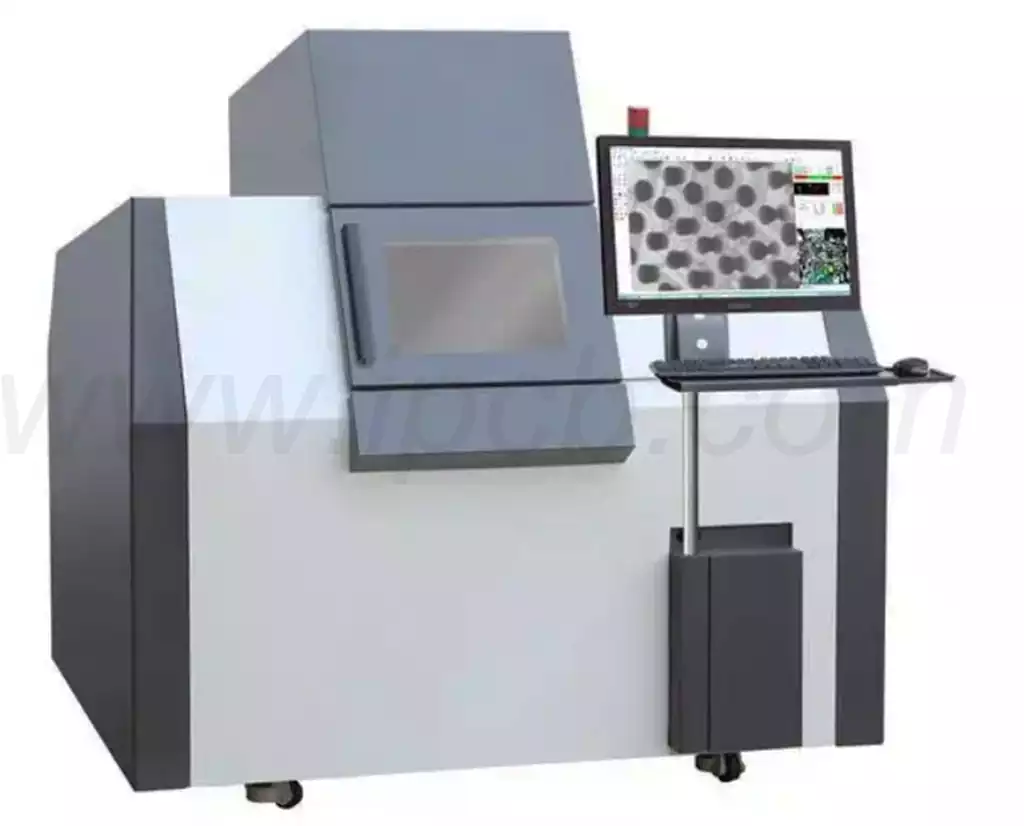
Impeccable chip-level reliability and compliance documentation: Every delivered BGA adapter board comes with a comprehensive, authoritative third-party quality documentation, including 100% TDR characteristic impedance measurement waveforms, precise metallographic microsection analysis of interlayer vias to prove the absence of any trace air gaps at the bottom of blind vias, and 100% automated optical defect inspection (AOI) and high-voltage insulation withstand voltage testing. Using iron-clad factory test data, we ensure that every fan-out high-speed signal line exhibits steel-like impedance and electrical stability under full-load high-frequency stress on the chip.