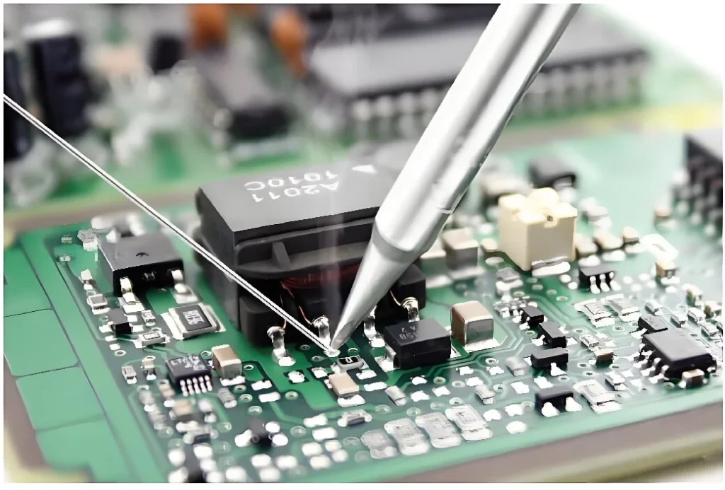
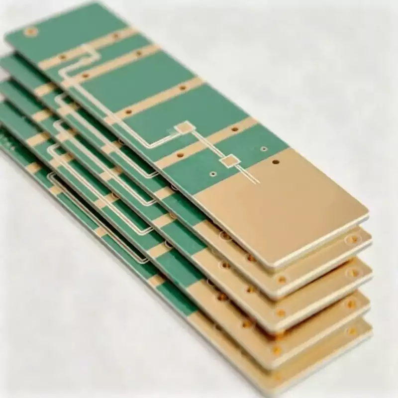
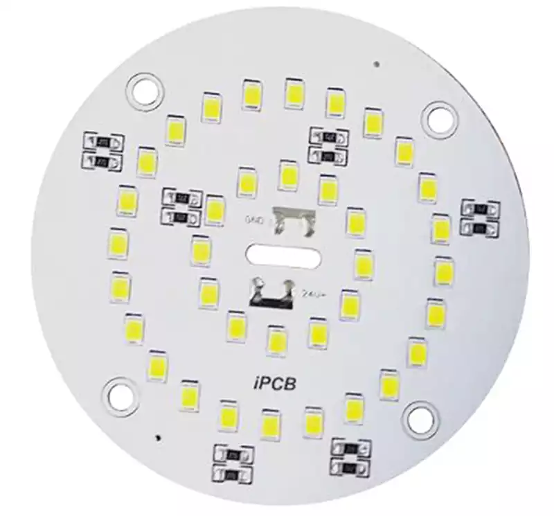
Millimeter wave pcbs are specialized circuit boards designed to operate at frequencies of 24 GHz, 28 GHz, 39 GHz, 60 GHz, 77 GHz, 79 GHz, and above. They have become one of the most critical foundational components in high-frequency electronics, supporting applications across five major sectors: 5G mobile communications, satellite communication systems, advanced driver assistance systems (ADAS) for automotive radar, high-speed interconnects for artificial intelligence computing, aerospace equipment, and advanced high-speed packaging modules.
From a PCB manufacturing perspective, millimeter wave pcb represent far more than an incremental improvement over conventional high-frequency circuit boards. They combine microwave engineering, ultra-precision manufacturing, advanced material science, and statistical process control into a highly sophisticated manufacturing discipline. Their production requires significantly higher standards for material performance, fabrication accuracy, and process consistency, making them fundamentally different from traditional high frequency PCB manufacturing.
The primary technical challenge of millimeter wave pcb technology stems from the extremely short wavelengths associated with millimeter-wave signals. As operating frequencies increase, signal wavelengths decrease dramatically, meaning that manufacturing variations measured in only a few micrometers can directly affect circuit impedance, signal phase, insertion loss, and overall RF performance.
The relationship between frequency and wavelength clearly illustrates this challenge. A 1 GHz signal has a wavelength of approximately 300 mm, while a 30 GHz millimeter-wave signal has a wavelength of only 10 mm. At the 77 GHz frequency commonly used in automotive radar, the wavelength is reduced to approximately 3.9 mm. Under these conditions, even minor variations in trace width, copper surface roughness, resin and fiberglass distribution, layer-to-layer registration, drilled hole positioning, surface finish quality, and fiberglass weave construction can significantly influence RF signal transmission performance.
As a result, the manufacturing philosophy for millimeter wave pcb differs fundamentally from that of conventional PCBs. Traditional boards primarily focus on electrical continuity, dielectric strength, and structural reliability, whereas millimeter wave pcb prioritize electrical performance consistency above all else. During design and manufacturing, engineers must precisely control impedance, signal phase, insertion loss, return loss, group delay, dielectric constant, dissipation factor, conductor surface transmission characteristics, and mode conversion to ensure reliable high-frequency performance.
The design of millimeter wave pcb reflects these demanding electrical requirements. Because dielectric loss and conductor loss are the two dominant factors affecting millimeter-wave signal transmission, selecting appropriate low-loss substrate materials is essential. The most widely used materials fall into two major categories. The first consists of polytetrafluoroethylene (PTFE)-based laminates, including Rogers RO3003, RO4350B, and RT/duroid materials. These laminates provide extremely low dielectric loss, highly stable dielectric constants, and outstanding high-frequency transmission characteristics, making them the preferred choice for premium millimeter-wave applications.
However, PTFE materials are mechanically soft, difficult to machine, challenging to drill, and possess relatively high coefficients of thermal expansion, resulting in extremely limited process tolerance during manufacturing. The second category consists of hydrocarbon ceramic laminates, including materials such as Megtron 6, Tachyon, and I-Speed. These materials provide excellent compatibility for designs combining high-speed digital signals with millimeter-wave RF transmission and offer greater manufacturing versatility.
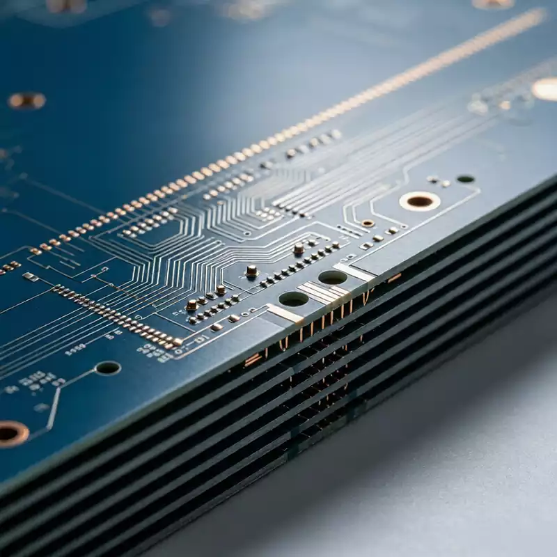
Copper foil selection is equally critical because millimeter-wave signals are strongly affected by the skin effect, with current flowing almost entirely along the conductor surface. At 30 GHz, for example, current penetrates only about 0.38 μm into the conductor. If the copper surface roughness reaches approximately 2 μm, signal transmission is significantly degraded and insertion loss increases substantially. Consequently, millimeter wave pcb manufacturing typically employs very low profile (VLP), hyper very low profile (HVLP), ultra-low profile (ULP), or reverse-treated foil (RTF) copper to minimize conductor losses and maximize transmission efficiency.
Trace geometry also demands exceptional manufacturing precision. At millimeter-wave frequencies, characteristic impedance becomes highly sensitive to conductor dimensions. Typical trace widths range from only 2 to 4 mil, while spacing is generally maintained between 2 and 3 mil. In ultra-high-frequency designs, trace widths may even fall below 2 mil. Achieving these dimensions requires highly controlled etching processes that carefully manage etch uniformity, lateral undercut, and trace edge quality, since even microscopic defects can result in unacceptable RF performance.
Transmission line design is another defining feature of millimeter wave pcb. The most commonly used structures include microstrip lines, stripline configurations, and coplanar waveguides with ground (CPWG). Among these, CPWG has become the preferred solution for many millimeter-wave applications because it offers superior electromagnetic interference suppression, stable impedance, convenient grounding, and reduced radiation loss. However, its manufacturing tolerance is extremely demanding. Even slight deviations in the spacing between signal traces and adjacent ground conductors, sometimes too small to trigger detection during automated optical inspection (AOI), may still prevent the completed assembly from meeting RF performance specifications.
To maintain precise impedance control, millimeter wave pcb frequently utilize ultra-thin core materials with thicknesses of 2 mil, 3 mil, or 4 mil. Although these thin laminates enable accurate impedance matching and stable signal transmission, they are mechanically fragile, prone to deformation, wrinkling, and registration errors during lamination, substantially increasing manufacturing complexity.
Via structures also assume a much more significant role than in conventional PCB designs. Rather than serving solely as electrical interconnections, vias become integral components of the RF transmission path. Back drilling is widely employed to eliminate via stubs that would otherwise generate resonance, signal reflection, and additional insertion loss at millimeter-wave frequencies. Filled vias and Via-in-Pad Plated Over (VIPPO) technology further improve impedance continuity while minimizing mode conversion, and via fencing is frequently incorporated to enhance electromagnetic shielding.
Surface finish selection is equally important for preserving RF performance. Conventional electroless nickel immersion gold (ENIG) finishes are generally avoided because the nickel layer introduces additional high-frequency transmission loss. Instead, millimeter wave pcb commonly use immersion silver, immersion tin, electroless nickel electroless palladium immersion gold (ENEPIG), or electroless nickel electroless palladium immersion gold with modified structures where appropriate. In some premium RF applications, protected bare copper finishes are selected to further reduce conductor loss and electromagnetic interference.
Manufacturing millimeter wave pcb presents numerous process challenges. PTFE and other high-frequency laminates differ substantially from conventional FR-4 materials. Their smooth surfaces, extremely low moisture absorption, limited surface adhesion, and susceptibility to thermal deformation make drilling particularly difficult, often resulting in defects such as resin smear, rough hole walls, nail-heading, and resin recession. Consequently, manufacturing yields are typically lower than those achieved with standard PCB materials.
Through-hole metallization presents another significant challenge because PTFE exhibits extremely low chemical activity. Conventional plating processes cannot reliably produce sufficient metal adhesion, leading to plating separation, blow holes, and poor bond strength. Plasma surface activation has therefore become a critical manufacturing process for increasing surface energy and ensuring reliable metallization inside drilled holes.
Multilayer lamination is equally demanding because many millimeter wave pcb combine PTFE with FR-4 in hybrid constructions. These materials exhibit substantially different coefficients of thermal expansion, resin flow behavior, and dimensional shrinkage characteristics. As a result, warpage, layer misregistration, and interlayer delamination become much more difficult to control during lamination.
Etching precision extends beyond simply achieving the specified trace width. At millimeter-wave frequencies, trace edge smoothness and sidewall quality become equally important because high-frequency current tends to concentrate along conductor edges. Even when AOI confirms that trace dimensions meet design specifications, excessive edge roughness may still cause RF performance to fail qualification testing.
Copper surface roughness also presents a difficult manufacturing trade-off. While minimizing conductor roughness effectively reduces insertion loss, insufficient surface treatment may weaken laminate adhesion, increase the risk of conductive anodic filament (CAF) formation, and reduce peel strength. Balancing electrical performance with long-term structural reliability remains one of the most challenging aspects of high-volume millimeter wave pcb production.
Impedance control requirements are considerably stricter than those for conventional circuit boards. Whereas standard PCBs generally permit impedance tolerances of ±10% and high-speed digital PCBs commonly require ±7%, millimeter wave pcb often demand impedance tolerances within ±3% to ±5%. Achieving this level of precision requires careful calibration of etching compensation, laminate dimensional stability, dielectric constant variation, copper thickness, and resin flow throughout the manufacturing process.
Another important consideration is the fiberglass weave effect. The dielectric constant of fiberglass is approximately 6.0, while the surrounding resin typically exhibits a dielectric constant near 2.3. This difference creates localized dielectric variations that can introduce signal phase errors and differential pair skew. To minimize these effects, millimeter wave pcb frequently employ spread-weave fiberglass, flat-weave constructions, or ultra-thin glass fabrics to improve dielectric uniformity across the laminate.
Successful production of millimeter wave pcb depends on comprehensive process control at every stage of manufacturing. Raw material consistency must be tightly managed by verifying the dielectric constant and dissipation factor of every laminate batch. High-volume production programs typically standardize suppliers, material batches, and resin content to ensure consistent electrical performance. Copper foil quality is controlled by monitoring surface roughness parameters such as Ra and Rz while maintaining consistent foil specifications across production lots.
Lamination processes rely heavily on statistical process control (SPC) to optimize heating rates, vacuum levels, pressure profiles, gel times, and resin flow, thereby minimizing thickness variation that could affect impedance. Drilling operations require strict control of hole wall quality, positional accuracy, and contamination through the use of new drill bits, optimized drill life management, and carefully selected entry materials. Etching processes focus not only on conductor dimensions but also on edge smoothness, sidewall geometry, and lateral etching characteristics to satisfy the demanding requirements of high-frequency RF transmission.
At millimeter-wave frequencies, manufacturing variations measured in only a few micrometers are sufficient to produce significant changes in RF performance. Achieving consistent high-volume production therefore depends on comprehensive process control throughout substrate preparation, precision etching, multilayer lamination, and through-hole metallization. Only by maintaining tight control over every critical manufacturing parameter can millimeter wave pcb manufacturers consistently deliver the electrical performance, reliability, and repeatability required for next-generation millimeter-wave applications.