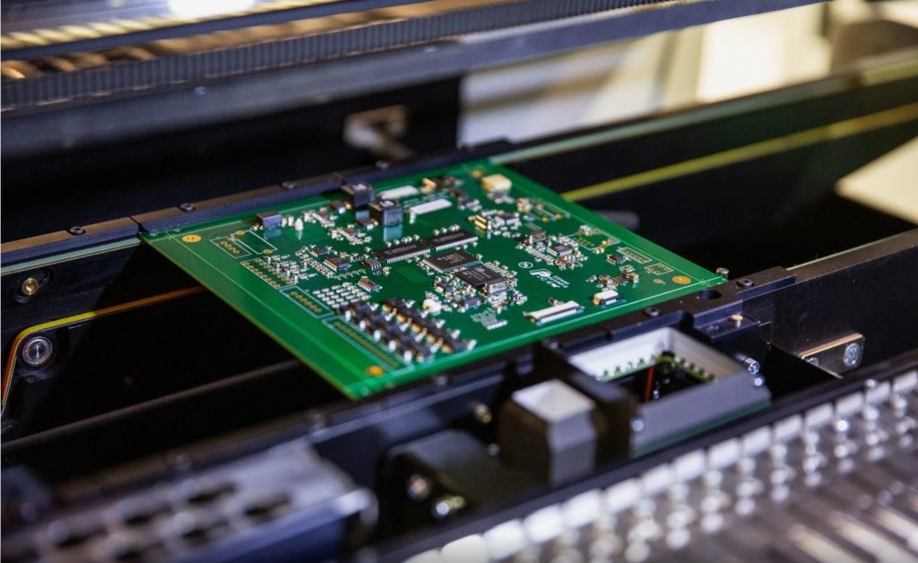
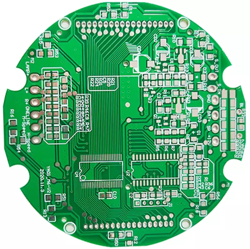
Small run PCB assembly is often treated as a simplified version of mass production. In practice, producing ten, fifty or several hundred reliable boards can be more difficult than running thousands of mature units. The manufacturer has fewer assemblies from which to absorb engineering time, stencil setup, programming, inspection and test-fixture costs. At the same time, the design may still be changing, components may be purchased in small quantities and the production process may not yet have stable parameters. The purpose of a small run is therefore not merely to obtain working boards. It should establish whether the design can be fabricated, assembled, inspected and tested repeatedly. When the build is controlled correctly, it becomes a bridge between prototype PCB assembly and volume production. When it is handled as an informal trial, unresolved design and process weaknesses can be carried directly into a larger order.
Small runs expose more manufacturing risk because a volume production line usually works with a released design, approved materials, validated assembly parameters and established test fixtures. A small run often begins before all these conditions exist. The BOM may contain temporary substitutions, firmware may still be under development and some components may have been selected according to prototype availability rather than long-term supply. These uncertainties interact with one another. Changing a voltage regulator may alter the thermal profile or startup sequence. Replacing a capacitor with the same nominal capacitance but a different dielectric can affect its effective value under DC bias. A connector substitution may fit the footprint while changing its mating height or pin strength. Because small run PCB assembly contains fewer units, a single defect can also produce a misleading yield result. If one board out of ten fails, the apparent defect rate is 10 percent, but the failure may have come from the design, a placement error, an incorrect component or an immature test method. The failure must be classified before the yield number has any useful meaning.
The production package must control one revision. Reliable manufacturing begins with a synchronized production package. Gerber or ODB++ data, drill files, stack-up requirements, BOM, centroid data, assembly drawings, schematics, firmware and test instructions must all describe the same hardware revision. Revision mismatches are particularly dangerous in small run PCB assembly because engineering changes often occur close to the build date. A PCB layout may be updated while the old centroid file remains in the production package. Firmware may expect a new boot resistor configuration that is not reflected in the assembly drawing. A substituted component may be added to the BOM without confirming its package dimensions. Every component should have a manufacturer part number rather than only a generic value. Descriptions such as “10 µF capacitor” do not define package size, voltage rating, tolerance, dielectric material or temperature characteristics. Approved alternatives should be documented separately, and each substitution should be reviewed for electrical, mechanical and manufacturing compatibility. Do-not-populate positions also need explicit control. Prototype boards often contain optional pull resistors, debugging headers and alternative communication circuits. The manufacturer should not have to infer which parts belong to a particular product version.
Component sourcing can control the entire schedule. Assembly time is rarely the only factor controlling delivery. For many low volume PCB assembly projects, component sourcing is the longest and least predictable stage. Small quantities may not qualify for normal distributor pricing, while tray, reel or moisture-sensitive packaging requirements can affect how components are purchased and handled. Some devices are available only in full reels, creating an excess-material cost that must be separated from the assembly price. Process losses should also be considered for very small passive components because the exact order quantity may not be sufficient for machine setup and placement. The risk is not limited to price. Components obtained through unauthorized channels may have uncertain traceability, storage history or authenticity. Moisture-sensitive ICs can appear normal during incoming inspection but develop package damage during reflow if they have not been stored and baked correctly. A controlled component sourcing process should therefore verify the exact manufacturer part number, authorized or traceable supply sources, date code and packaging condition, moisture sensitivity requirements, minimum purchasing quantity, approved alternatives and their validation status. This information allows purchasing decisions to be made before the production schedule is committed. It also distinguishes reusable inventory from material that belongs only to the current hardware revision.
DFM review prevents expensive setup failures. A DFM review for small run PCB assembly should examine whether the board fits the manufacturer’s actual fabrication and assembly process. Passing a general design-rule check is not enough. Fine-pitch components need appropriate solder-mask openings and paste-aperture design. Components placed too close to the board edge may interfere with panel rails or depanelization. Heavy connectors and large thermal pads may require different paste strategies from nearby miniature components. If both appear on the same side of the board, a single stencil thickness may not provide an adequate process window for every joint. BGA escape routing, via structures, copper balance and board thickness can also affect fabrication yield. A board that uses theoretical minimum dimensions may be possible to fabricate but difficult to reproduce consistently. The design should use the most demanding feature only where it provides a necessary electrical or mechanical benefit. Test access must be reviewed at the same time. Adding test points after the layout has been completed often produces poor probe access or unwanted stubs on sensitive signals. Power rails, ground, reset, programming connections and important communication interfaces should have an intentional test strategy before manufacturing files are released.
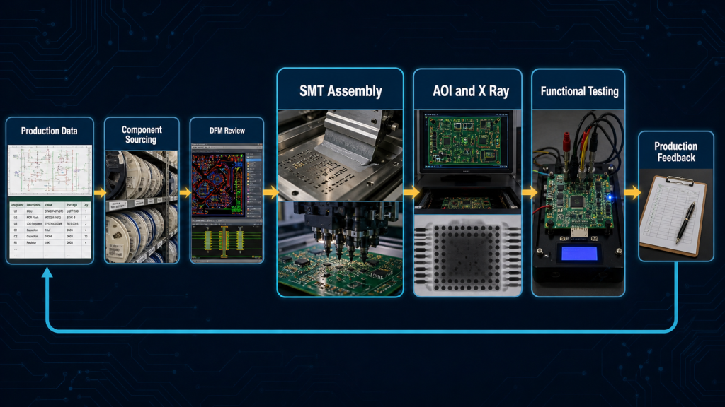
Solder paste and reflow need product specific control. Small quantities do not remove the need for a controlled SMT process. Solder-paste printing remains one of the largest contributors to assembly defects, especially for fine-pitch ICs, bottom-terminated components and BGAs. Paste volume must be sufficient to form reliable joints without creating bridging or component float. Thermal pads may require segmented apertures to manage solder volume and outgassing. Very small passive components need balanced deposits to reduce tombstoning, while large connectors may need additional solder that cannot be achieved by simply increasing paste across the entire board. The reflow profile should reflect the thermal mass of the actual assembly. A temperature measured in the reflow oven is not automatically the temperature experienced by the solder joints. Large copper areas, shields, connectors and power components can heat more slowly than surrounding devices. For a new small run PCB assembly project, profile verification is more valuable than relying on a generic oven recipe. Thermocouples should be placed at thermally significant locations, including dense component areas, large ground-connected pads and packages with critical temperature limits. Once verified, the profile becomes part of the manufacturing record and provides a starting point for subsequent orders.
Inspection must match the hidden defect risk. Automated optical inspection can identify polarity errors, missing components, placement offsets and many visible solder defects. It cannot directly inspect solder joints hidden under BGAs, QFNs or other bottom-terminated packages. X-ray inspection is appropriate when hidden joints create a significant reliability risk. It can reveal bridging, missing solder, alignment problems and abnormal voiding. However, X-ray does not prove that every joint is electrically continuous or mechanically durable. Inspection results must be considered together with paste control, reflow data and electrical testing. First-article inspection is especially important. Before the complete batch proceeds, the first assembled boards should be checked against the BOM, drawings and polarity requirements. Critical package orientation, connector position and mechanical dimensions should be confirmed before the process produces the remaining units. This approach prevents one programming error, rotated component or incorrect substitution from affecting the entire order.
Functional testing should reproduce real failure conditions. A board that powers on is not necessarily a functioning product. Effective PCB assembly testing must exercise the circuits most likely to reveal manufacturing defects. The test sequence may begin with resistance checks and controlled current-limited power application. Supply rails, startup current, reset behavior and programming access can then be verified before full functional testing. The next stage should exercise memory, communication ports, sensors, displays, audio channels, motor outputs or other product-specific functions. Testing should be designed around failure mechanisms rather than convenience. An Ethernet interface should transfer data instead of merely reporting a link. Storage should complete read-and-write operations. A motor-control board should be tested under a representative load, and a wireless product should demonstrate communication performance in a defined configuration. In small run PCB assembly, test results also provide engineering information. Repeated failures on the same interface may indicate a design-margin problem rather than random workmanship. Recording the serial number, hardware revision, firmware version and test outcome makes that pattern visible.
A golden sample is useful but not sufficient. An approved golden sample helps operators confirm assembly appearance, connector orientation and basic behavior. It can also provide a comparison unit during functional testing. However, the sample should not replace controlled documentation. A physical board cannot show the approved component source, paste-aperture specification, firmware checksum or acceptable electrical limits. It may also contain manual modifications that were never incorporated into the production data. The released drawings, BOM and test specification must remain the primary manufacturing authority. The golden sample should support those documents, not override them.
How the first run prepares the product for production. The most valuable output from a small run is not only the delivered hardware. It is the manufacturing knowledge produced during the build. Defects should be separated into design, material, assembly, programming and testing categories. Rework instructions must be documented, and any recurring manual correction should trigger a design or process review. Changes made during the build need to be incorporated into the next controlled revision rather than retained in email messages or operator notes. Yield data should also be interpreted carefully. A high final yield achieved after extensive rework does not indicate a stable process. First-pass yield provides better evidence of whether the production package and assembly controls are mature. For customers moving from engineering samples toward repeatable production, iPCB can combine fabrication review, component sourcing, PCBA, inspection, programming and functional testing within one revision-controlled workflow. This reduces the risk of design, material and test information becoming disconnected between suppliers.
A successful small run produces a repeatable process. Small run PCB assembly succeeds when the finished boards work and the manufacturer can explain why the process worked. Controlled production data, traceable components, verified soldering parameters, appropriate inspection and product-specific functional testing turn a limited build into useful production validation. The final objective is not to imitate mass production at a smaller quantity. It is to expose manufacturing weaknesses while changes are still affordable. When every defect, substitution and test result is connected to the correct hardware revision, small run PCB assembly provides the evidence needed to increase production volume without carrying hidden risks into the next order.