In the vast landscape of modern electronics manufacturing, from miniature smart wearable devices to high-density server motherboards, hundreds of millions of electronic products rely on the precision support of printed circuit boards (PCBs). However, in automated surface mount technology (SMT) production lines, chemical copper plating baths, and high-speed flying probe testing machines, individual small circuit boards are almost never directly handled. Instead, the vast majority of circuit boards exist in a strictly designed array form during the manufacturing and assembly stages—this is the PCB panel boards.
A panel board is far more than simply piecing together multiple circuit boards onto a large board. It is a crucial bridge in electronic manufacturing engineering (DFM) connecting physical materials, automated robotic arms, thermodynamic stress control, and high-density electromagnetic topology. Panel board design directly determines bare board manufacturing costs, surface mount technology (SMT) soldering yield, mechanical depaneling stress damage rate, and long-term operational physical reliability.
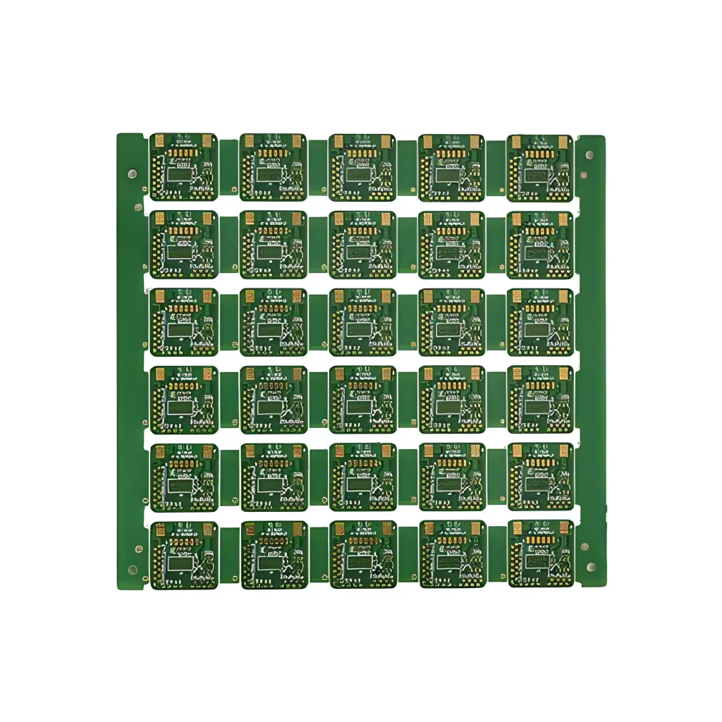
The Physical Essence and Logic of Large-Scale Manufacturing of Panel Boards
To understand the engineering value of panel boards, we must first discuss the physical limitations of circuit board raw materials and the automation logic of the surface mount technology industry.
Substrate Utilization and Standardized Physical Dimensions
The basic materials for circuit boards (such as FR-4 fiberglass epoxy copper-clad laminate, polyimide flexible substrate, or high-frequency ceramic substrate) arrive at the factory in the form of standardized giant motherboards (often called large copper-clad laminates). Common industrial motherboard dimensions have strict physical specifications.
If individual boards of varying shapes and tiny sizes are processed directly, a large amount of scrap material is generated at the edges of the motherboard. The first physical logic of panelization technology is to use algorithmic geometric arrangement to lay dozens or even a few individual boards in an optimal physical topology within the large board space, maximizing substrate utilization. In modern PCB manufacturing, every few percentage points increase in substrate utilization translates to millions in reduced raw material procurement costs in large-scale mass production.
Physical Transmission and Clamping in Automated SMT Placement Lines
On SMT placement production lines, high-speed placement machines, solder paste printers, and reflow ovens rely on conveyor belts to transport the boards. Automated robotic arms apply tremendous physical impact to boards during high-speed placement processes involving tens of thousands of points per hour.
Small or irregularly shaped boards (such as round, L-shaped, or polygonal boards) cannot be smoothly transported on standard conveyor tracks and lack sufficient edges for mechanical fixtures to position and hold them. Panelization, by adding standard process edges (Panel Edges) around the perimeter, uniformly wraps various irregularly shaped boards into standard rectangular panels with symmetrical structures and flat edges. This eliminates the need for frequent adjustments to track widths and fixture parameters for each specific product in automated production lines, achieving standardization and high speed in the electronics manufacturing industry.
Panel Structure Anatomy: Process Edges, Positioning Holes, and Optical Markers
A qualified panel is a micro-engineered system containing the main circuit area and various auxiliary manufacturing structures.
Process Edges: Mechanical Support and Automated Conveyor Belts
Process edges are the guiding and supporting areas surrounding the outermost part of the panel. Their width is typically set between a few millimeters and tens of millimeters, depending on the requirements of the automated equipment.
The primary responsibility of the process edge is to withstand belt friction and fixture pressure during SMT transport, while preventing the guide rail from colliding with sensitive components on the board edges. In the high-temperature environment of reflow or wave soldering, the process edge also maintains the structural rigidity of the entire panel, preventing severe physical sagging and thermal deformation at temperatures exceeding 200 degrees Celsius.
Positioning Holes and Optical Mark Points: A Physical Coordinate System for Micron-Level Alignment
The four corners of the panel’s process edge are covered with meticulously designed holes and metallic patterns, serving as the physical coordinate reference system for automated equipment to identify the space.
Mechanical positioning holes provide physical pin-like mechanical positioning in flying probe testing, bed-of-needle testing, and automated depaneling machines, ensuring precise board positioning.
Optical Mark Points are a set of conductive copper dots with micron-level precision, typically treated with maskless gold plating or immersion tin, surrounded by a contrast area without solder resist ink. When reading a panel, the high-speed vision camera of an SMT pick-and-place machine first scans these Mark points. Image recognition algorithms calculate the panel’s offset, tilt angle, and even minute deformation in three-dimensional space, then automatically correct the placement head’s position. Without these physical Mark points, high-density chips with micron-level pin pitch (such as BGA or QFN packages) simply cannot be accurately placed on the pads.
Segmentation and Separation Engineering: The Microphysics of Connection and Disassembly
The core contradiction of a panel lies in the fact that it must maintain robust physical integrity during processing and soldering, while simultaneously being easily and non-destructively cut and separated into individual boards after assembly. To address this, engineers have invented various micro-segmentation physics techniques.
V-Cut Process: Stress Concentration and Fracture Control
V-Cut is the most common panel segmentation technique. It involves using a high-precision circular diamond saw blade to cut a V-shaped groove approximately one-third the thickness of the board on both sides, leaving a thin “core” in the middle. The physical essence of V-Cut technology utilizes the principle of stress concentration in fracture mechanics. After all components are soldered onto the panel, the operator or depanel applies bending force along the V-groove. All mechanical stress is instantly concentrated at the weakest point of the V-groove, causing the board to fracture smoothly along a pre-set straight line.
The advantage of V-Cut is its smooth cut edge and the fact that it does not occupy additional physical spacing between boards (adjacent boards can share a single V-groove). However, its limitations are also significant: the cut must be an absolute straight line running through the entire panel, making it impossible to handle curved edges; furthermore, if the residual stress from the V-groove cutting is not properly released during depaneling, it can easily cause ceramic cracking in the micro-layer capacitors (MLCCs) close to the V-groove edge, leading to serious electrical short circuits.
Stamp Holes & Breakaway Tabs: Micro-perforation Networks for Curved and Irregularly Shaped Boards
For non-rectangular circuit boards with complex outlines, V-Cut cannot cut curves; in such cases, “stamp hole” connection technology must be used.
The process of creating “stamp-shaped perforations” involves first using a CNC milling cutter to hollow out the insulating substrate between adjacent veneers, leaving only a few millimeter-wide tiny connecting bridges (called breakaway tabs). Then, a row of tiny through-holes is drilled into these connecting bridges using a micro-drill. This row of holes closely resembles the perforations on the edge of a stamp, hence the name “stamp-shaped perforations.”
Stamp-shaped perforations weaken the local bending strength of the connecting bridges by utilizing these tiny through-holes. During separation, cracks propagate along the perforations, eventually breaking the connecting bridges. This method is highly adaptable and can be arranged around any complex curved contour. However, after breakage, tiny burr residue remains on the veneer edges, typically requiring subsequent manual grinding or a second CNC milling.
CNC milling grooves and anti-flying plate supports: In high-end panelizing requiring extremely high edge flatness and no residual stress, factories use high-speed rotating CNC milling cutters to almost completely mill through the veneer insulating substrate, leaving only tiny support points at critical stress nodes. To prevent PCBs detached during milling from flying off in high-speed winds and damaging components, anti-flying supports and specialized fixtures are incorporated into the panel design.
Thermodynamics, Electromagnetism, and Stress Game in Panel Design
Panel design is not simply a geometric arrangement; it involves extremely complex interplay of physics and materials science. An improper panel design can cause an entire batch of circuit boards to be instantly scrapped upon entering the reflow oven.
Mismatched Coefficients of Thermal Expansion (CTE) and Thermal Torsion
Circuit boards are composed of fiberglass, epoxy resin, and copper foil. These materials exhibit significant physical differences in their coefficients of thermal expansion.
During reflow soldering, the temperature rapidly rises from room temperature to over 240 degrees Celsius, and the molten solder holds the components to the board. If the copper foil distribution on the panel is extremely uneven (e.g., a large area of ground copper on the left side of the panel, while the right side has sparse, thin traces), a severe asymmetry will occur in the heat absorbed and the rate of thermal expansion on both sides. This thermal stress difference causes severe warping and twisting of the entire panel at high temperatures.
Warped panels cannot return to flatness after cooling, leading not only to poor soldering or bridging of BGA solder balls but also to inaccurate positioning by automated depaneling machines. Therefore, panel design must pursue strict “electromagnetic and copper foil symmetry.” In blank areas without signal traces, engineers must manually add a grid of auxiliary balancing copper foil to ensure that the thermal resistance and thermal expansion of the entire panel remain consistent.
The Thermal and Production Efficiency Revolution of Mirror/Top-Bottom Panelization
To pursue ultimate production efficiency, a design called “mirror panelization” (or mirror panelization) has been widely adopted.
In traditional panelization, all individual boards face up and down. Mirror panelization, however, flips adjacent boards 180 degrees, forming a mirrored arrangement of opposite sides.
The Yin-Yang board brings two significant engineering advantages:
Double SMT production line efficiency: Previously, two separate production lines or two program adjustments were needed to solder the front and back sides. With the Yin-Yang board, the same production line, the same placement program, and the same stencil can simultaneously print and place both sides of the circuit board. After the first reflow, the panel can be flipped over and reflowed again, producing a complete finished product in one pass.
Extremely balanced thermal mass distribution: The Yin-Yang board physically complements the high-density chip area with the low-density passive component area, resulting in an extremely uniform heat mass distribution across the entire panel during reflow soldering, greatly suppressing board deformation caused by localized overheating.
Control of center of gravity shift and component ejection: In irregularly shaped panels, if the individual boards are arranged too haphazardly, it can cause a significant shift in the panel’s physical center of gravity. When the placement head of a high-speed pick-and-place machine moves above the panel with extremely high acceleration, the unstable center of gravity of the panel will cause micro-vibrations in the physical fixtures of the transport track. This high-frequency micro-vibration can cause displacement or even detachment of micro-components (such as 0201 packaged resistors) that have been precisely placed on solder paste but not yet soldered, resulting in a huge component rejection rate and high defect rate.
Special Panel Topologies: Flexible Boards, Rigid-Flex Boards, and High-Frequency Boards
As electronic devices become thinner, more flexible, and utilize high-frequency communication, traditional rigid FR-4 panel engineering faces entirely new physical challenges.
Flexible Circuit Board (FPC) Tension and Carrier Panelization
Flexible circuit boards use extremely thin polyimide film as the substrate, which itself has no mechanical rigidity, much like a soft plastic film.
During panelization, flexible boards cannot be directly transported on the SMT track belt using their own process edges like rigid boards. Therefore, flexible panels must utilize dedicated “magnetic carriers” or “skin mounting fixtures.” Before processing, flexible panels are tightly bonded to a rigid metal or synthetic stone carrier using high-temperature resistant tape or positioning pins to force flatten the surface. After all patch soldering is completed, they are peeled off from the carrier. The connecting bridge design of the flexible panel must also be more gradual to prevent tearing of the fragile polyimide substrate during disassembly.
Rigid-Flex Spatial 3D Panelization: Rigid-flex panels integrate rigid and flexible circuit boards together to achieve connectorless folding assemblies in complex three-dimensional spaces (such as the hinge area of foldable screen phones).
The panel design of rigid-flex panels is the most challenging in all PCB manufacturing processes. Due to the orders of magnitude difference in thickness, material stiffness, and thermal expansion rates between the flexible and rigid areas, the panel must establish a robust protective frame around the rigid area while reserving sufficient physical deformation buffer grooves in the flexible folding area. Slight mishandling can cause the thermal stress during high-temperature soldering to generate enormous shear forces at the rigid-flex interface, leading to tearing of the internal copper foil.
Microwave Shielding and Edge Effects in High-Frequency RF Panels
In high-frequency fields such as 5G millimeter-wave communication and millimeter-wave radar, the physical structure of the panel can even affect the distribution of microwave electromagnetic fields.
If the process edge of a high-frequency panel is too close to the microstrip line or antenna on the motherboard, the copper foil on the process edge will electromagnetically couple with the high-frequency antenna, changing the antenna’s resonant frequency and radiation pattern. Furthermore, the irregular physical edges cut by the V-Cut saw blade can cause stray scattering of high-frequency electromagnetic waves at the edges. Therefore, high-frequency panels not only require burr-free physical separation, but also necessitate a sufficiently wide “electromagnetic clearance zone” between the process edge and the signal area, and a dense network of grounded shielded vias along the process edge.
Automated Separation Engineering and Quality Control
After the panel has successfully passed solder paste printing, surface mount technology (SMT), reflow soldering, and optical inspection (AOI), the final step in the panel’s mission is to safely “separate” these individual boards, which are already covered with sensitive components.
Stress Sensitivity and the Evolution of Automated Depaneling Equipment
Early manual depaneling by hand is a taboo in modern electronics manufacturing. The torsional stress applied by manual bending generates unpredictable stress waves within the board, causing cracks in the solder joints of surface-mount leadless chips or internal microcracks in high-dielectric-constant capacitors. This latent damage often goes undetected during factory testing but can suddenly cause malfunctions after several weeks of user use.
Modern electronics manufacturing widely employs low-stress automated depaneling equipment:
Rotating and Circular Cutting Machines: Specifically designed for V-Cut panelization. Using a precision-aligned circular cutter, it smoothly rolls along the V-groove, minimizing stress concentrated at the V-groove and preventing severe breakage.
Router Milling Machines: Use high-speed rotating micro-milling cutters (reaching tens of thousands of revolutions per minute) to precisely cut connecting bridges along stamp-hole or milling groove paths. The equipment is equipped with a powerful negative pressure dust extraction system that removes glass fiber dust generated during cutting in real time, preventing dust contamination of sensitive optical components or miniature sensors.
Laser Depaneling: Currently the most advanced stress-free depaneling technology. Utilizing high-energy-density ultraviolet or ultrafast picosecond/femtosecond laser beams, it directly breaks the molecular bonds between the insulating substrate and metallic copper, achieving contactless evaporation cutting. The laser depaneling process is completely stress-free, producing extremely clean cuts. It can perform micron-level cutting close to component edges, making it the ultimate depaneling solution for high-density microelectronic devices.
Strain Gauge Testing and Panel Depanel Quality Assessment
To ensure that the panel depaneling process does not damage expensive circuit boards, high-end electronics manufacturing requires “quantitative measurement of physical stress” during the depaneling process.
Engineers glue extremely small “resistance strain gauges” close to sensitive areas such as panel dividers, BGA chips, and large capacitors. The strain gauges convert minute physical deformations (microstrain) occurring on the board into changes in resistance in real time and input them to a high-speed strain gauge.
By plotting the stress-time curve at the moment of depaneling, engineers can accurately assess whether the physical cutting force of the current depaneling machine exceeds the critical safety stress limit allowed by the chip (typically required to be controlled within a few hundred microstrains). Once the limit is exceeded, the cutting speed of the depaneling machine, the tool sharpness, or the topology of the panel’s interconnect bridges must be adjusted immediately.
Summary
Printed circuit board panelization is not an isolated geometric design task. It is a comprehensive physical entity in electronic manufacturing engineering that spans materials science, mechanical dynamics, thermodynamics, and electromagnetics.
From the micro-cutting utilization rate of copper-clad laminates to the high-speed optical coordinate positioning of SMT pick-and-place machines; from the thermal-mass symmetry balance of the motherboard to the zero-stress micro-fracture of laser-driven depaneling, panelization spans the entire lifecycle of electronic products, from design drawings to physical devices.
With the continuous advancement of miniaturization, high-density interconnect (HDI), and heterogeneous integration technologies, future panelization design is evolving towards greater intelligence, three-dimensionality, and extreme stress control. A deep understanding and mastery of the physical mechanisms behind panelization is an essential foundation for achieving high-yield, low-cost, and high-reliability mass production in the modern electronics industry.