PCB board edge connectors can pass initial electrical testing and still develop intermittent contact after months of insertion, vibration or temperature cycling. The fault may appear as a momentary signal interruption, unexplained system reset, communication error or local temperature rise at a power contact. These failures are difficult to diagnose because the connection often recovers after the card is removed and inserted again. Reinsertion changes the physical contact position and temporarily wipes contamination from the gold fingers. By the time the board reaches a repair bench, it may operate normally again. Understanding the failure requires examining the entire contact interface rather than testing the PCB and connector separately.
Contact resistance changes at a microscopic level. A connector contact does not touch the entire visible gold finger. Even polished metal surfaces contain microscopic peaks and valleys. Electrical current passes through a limited number of small contact points where the spring contact applies pressure. When PCB board edge connectors are new, these points usually provide stable electrical continuity. Repeated insertion, vibration and environmental exposure gradually change the contact surface. Wear can remove part of the protective plating, while small movements can introduce oxides or debris between the mating surfaces. The resulting increase in contact resistance may be too small to detect with a basic continuity test. Under operating current, however, the affected connection can generate heat or produce a voltage drop. Low-level signals may experience data errors even when no visible damage is present. The problem is therefore not always a completely open circuit. Many field failures begin as a small and unstable change in resistance.
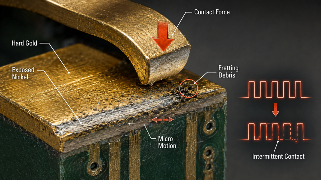
Plating wear exposes the underlying metal. PCB gold fingers need a finish capable of surviving the expected number of mating cycles. Hard gold is commonly applied over a nickel barrier because the gold resists corrosion while the nickel limits diffusion and supports the contact surface. If the gold layer is unsuitable or wears through, the connector can reach the nickel or copper below it. These exposed materials oxidize more readily than gold. Contact resistance then becomes sensitive to humidity, contamination and mechanical movement. An ordinary solderable finish should not automatically be treated as a durable contact finish. ENIG provides a flat surface for component assembly, but its gold layer is not intended to provide the same repeated-wear performance as a specified hard-gold contact surface. Samtec recommends cobalt-hardened gold for edge-card contacts and matching PCB pads in applications involving substantial mating cycles. The company also notes that the plating system must be considered together with contact force and connector use. For PCB board edge connectors, the production drawing should state the approved plating material, thickness and contact area. A note that says only “gold fingers” does not define enough information to control long-term wear.
Fretting can occur without full insertion cycles. Connector wear is not limited to deliberate insertion and removal. Vibration, thermal expansion and mechanical movement can cause tiny repeated motions between the socket contact and the PCB gold finger. This movement is called fretting. It can remove protective surface material and generate small wear particles. When the underlying metal is exposed, these particles can oxidize and accumulate inside the contact area. Fretting corrosion may create intermittent faults even when the card has never been intentionally removed. Industrial equipment, vehicles, motors and products with repeated heating and cooling are particularly exposed to this failure mechanism. Molex identifies vibration and shock as causes of micro-motion and fretting at connector interfaces. It also notes that insufficient contact pressure increases vulnerability to resistance changes and signal dropouts. PCB board edge connectors should not carry the mechanical load of the complete card. Guide rails, latches, screws or enclosure supports need to prevent movement after mating. The connector maintains electrical contact, while the mechanical structure restrains vibration and card motion.
Contamination interrupts the contact interface. Dust, flux residue, oil and handling contamination can enter the mating area. Even a thin film can reduce the number of microscopic points carrying current. Gold fingers are sometimes touched during manual assembly because their surface looks mechanically robust. Fingerprints introduce oils and salts that may attract moisture or contribute to corrosion. Packaging materials can also leave residue if the contact edge is not protected during transport. Flux creates a different risk. If soldering or manual rework occurs close to the edge connector, airborne residue can settle on the fingers. Cleaning the general PCB surface does not guarantee that the mating region is free of contamination. The contact-wipe action may remove light surface films, which explains why reinserting the card often restores operation. This recovery is temporary when the contamination remains inside the connector housing. Production handling should protect PCB board edge connectors from direct contact. Inspection, cleaning and packaging methods should treat the gold fingers as precision contact surfaces rather than ordinary copper pads.
Incorrect card thickness changes contact force. Every edge-card socket is designed for a specified PCB thickness range. A board near the upper limit creates more contact deflection and insertion force. A board below the permitted thickness produces less normal force against the gold fingers. Insufficient force makes the connection more sensitive to vibration and contamination. Excessive force can accelerate plating wear, deform contacts or damage the connector housing. The finished thickness of the PCB includes laminate, copper and surface processing. Variation across the board edge may also affect how evenly the contacts engage. For this reason, nominal board thickness alone does not prove compatibility. When intermittent failures affect many positions across the same card, thickness or alignment should be investigated before assuming that every contact is independently contaminated.
Poor alignment creates uneven wear. A board entering at an angle may engage one side of the connector before the other. Contact tips can scrape the edge of the gold fingers, while some positions experience greater deflection than intended. Damage may appear as narrow scratches, exposed nickel or wear concentrated on one side of each finger. Repeated misalignment can also deform socket contacts, creating a fault that remains even after the PCB is replaced. Bevel geometry helps guide the contact onto the plated surface, but the bevel cannot correct an enclosure that allows excessive angular movement. The chassis, card guide and connector must align the board before significant insertion force reaches the contacts. Polarization features are also important. A slot, key or asymmetric edge prevents reversed insertion and limits the possibility of contacts landing between fingers. For PCB board edge connectors used in serviceable products, mechanical alignment should remain consistent after repeated maintenance. A board that requires the technician to push sideways while inserting it is already placing uncontrolled load on the interface.
High speed failures may look like software problems. High-speed interfaces can fail before a conventional resistance measurement reveals an obvious contact problem. Local wear, contamination or reduced normal force changes the electrical transition between the PCB finger and connector contact. The result may be increased loss, reflections or crosstalk. A communication link can retrain at a lower speed, report occasional data errors or fail only at elevated temperature. Restarting the equipment may temporarily restore operation, making the fault appear related to firmware. When several high-speed channels pass through the same connector, compare error patterns by lane or contact position. A failure that follows one physical contact after board substitution points toward the socket. A failure that follows the removable card suggests the gold finger, card geometry or associated PCB routing. The diagnosis should preserve the condition of the interface. Cleaning or repeatedly reinserting the card before inspection can remove evidence and make the original failure difficult to reproduce.
Diagnosing an intermittent edge connection. Troubleshooting should begin by recording when the failure occurs. Temperature, vibration, operating current, card position and time since insertion can reveal whether the problem is electrical, mechanical or environmental. The gold fingers should be inspected under magnification for scratches, uneven wipe marks, discoloration and exposed base metal. A normal wipe pattern is consistent across comparable contacts. A pattern concentrated near one edge suggests incorrect insertion depth or alignment. The socket should also be inspected. A damaged or recessed contact may not apply the same force as the surrounding positions. Debris inside the housing can be difficult to see without suitable lighting and magnification. Contact resistance should be measured without allowing the test procedure to disturb the interface. For signal connections, operational error monitoring may reveal instability more effectively than a simple continuity check. Power contacts should also be checked for localized temperature rise under representative current. Molex connector validation includes contact-resistance monitoring, vibration, mating cycles and inspection for visible fretting or exposed base metal. These methods demonstrate why a single room-temperature continuity test is insufficient for an intermittent connector fault.
Production control prevents repeat failures. A corrective action should address the actual failure mechanism. Cleaning may resolve contamination but cannot restore worn plating. Replacing a socket may correct a deformed contact but will not prevent recurrence if the enclosure continues to misalign the card. Manufacturing records should connect failures to the PCB lot, plating batch, connector lot and assembly date. If multiple boards show similar wear positions, the cause is more likely related to geometry, thickness or mechanical alignment than random surface damage. For products using PCB board edge connectors, iPCB can review gold-finger plating, finished card thickness, bevel quality, panel processing and mating-area inspection during PCB manufacturing. These controls help ensure that the removable card matches the connector specification before it enters system assembly. Environmental and mechanical validation should then represent the real application. Required tests may include repeated mating, vibration, thermal cycling, contact-resistance monitoring and inspection of the wear surface. Testing should reproduce the expected product life rather than only prove that a new connector works.
Stable contact depends on more than gold fingers. Intermittent failures in PCB board edge connectors usually develop through a combination of surface wear, insufficient contact force, contamination and uncontrolled card movement. Reinsertion may temporarily restore operation, but it does not remove the underlying cause. A durable interface requires compatible plating, controlled finished thickness, consistent alignment and mechanical support after mating. Inspection and testing must examine resistance stability and wear rather than relying only on initial continuity. When the connector, PCB edge and enclosure are treated as one contact system, PCB board edge connectors can maintain stable electrical performance through repeated insertion and long-term operation.