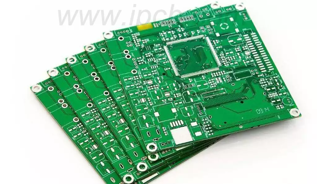
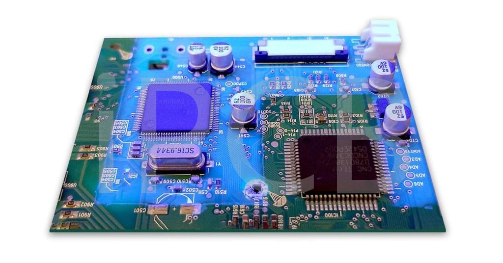
HDI PCBs are high-end, high-density interconnect printed circuit boards that combine multilayer stackup architectures with precision interconnect technologies to meet the development requirements of miniaturized electronic products and high-speed signal transmission.
Unlike conventional multilayer PCBs, which primarily increase the number of copper layers to provide additional routing space, HDI PCBs rely on laser-drilled microvias, blind and buried vias, fine-line circuitry, and sequential lamination to shorten signal paths and increase routing density. This technology is widely used in fine-pitch BGA devices, communication modules, automotive electronics, and various compact smart devices. Many engineers mistakenly assume that HDI PCBs are simply multilayer PCBs with a higher layer count. In reality, via structures, dielectric material selection, layer-to-layer registration accuracy, and the lamination process are the factors that have a major impact on manufacturing yield, reliability, and electrical performance.
HDI PCBs vs. Conventional Multilayer PCBs
The fundamental difference between HDI PCBs and conventional multilayer PCBs lies in their interconnect technologies and routing strategies rather than simply in the number of PCB layers.
Conventional plated through-hole technology is mature and reliable, with well-controlled manufacturing costs, making it suitable for most standard electronic products. However, as the pin pitch of semiconductor packages continues to decrease, the relatively large footprint of through-holes becomes an increasingly significant limitation.
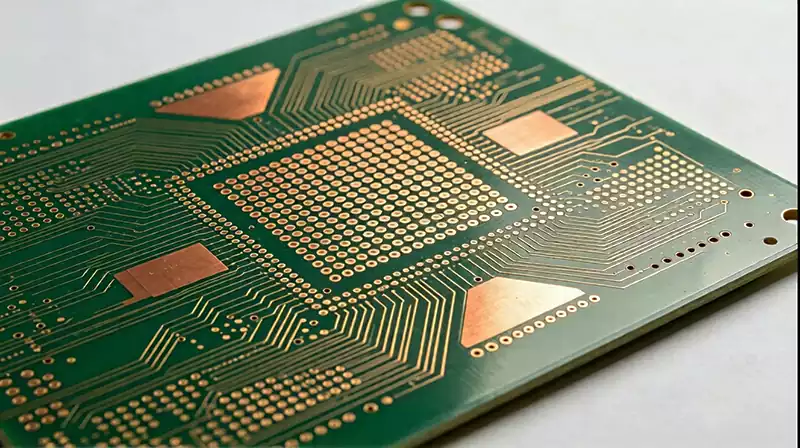
In fine-pitch BGA areas, conventional through-holes can occupy a considerable amount of routing space, making it difficult to fan out signals from the BGA pads. HDI PCBs use microvias to directly connect surface pads to adjacent inner layers, while blind vias terminate at designated target layers and buried vias are located entirely within the inner-layer structure. This configuration makes more efficient use of the available routing resources.
For ultra-high-density layouts, via-in-pad technology can also be used to place microvias directly within component pads. After the microvias are copper-filled and planarized, the pad surface remains sufficiently flat for reliable solder paste printing and SMT component placement. With a properly optimized HDI structure, it may even be possible to reduce unnecessary layer stacking and control the overall manufacturing cost.
Microvias in HDI PCBs
Microvias are one of the most critical structures in HDI PCBs. They are formed by precision laser drilling through thin dielectric layers, providing a level of dimensional and positional accuracy that is significantly higher than that achievable with conventional mechanical drilling.
Because of their small diameter, microvias can be positioned near the edges of component pads or directly within the pads, helping resolve routing constraints around high-density components where conventional vias would consume too much available space.
Microvia structures are generally classified into staggered and stacked configurations. In a staggered microvia structure, microvias on different layers are offset from one another rather than vertically aligned. This configuration helps reduce the risk of failures caused by thermal-mechanical stress and generally provides better manufacturing yield, making it suitable for many conventional high-density applications.
In a stacked microvia structure, microvias on multiple layers are vertically aligned to form a continuous interconnection through the buildup structure. This approach provides higher routing density and greater design flexibility, but it also imposes much stricter requirements on copper filling uniformity, layer registration accuracy, and thermal reliability. Therefore, the appropriate microvia structure should be selected by balancing the actual routing requirements against the manufacturing capabilities of the PCB fabricator rather than simply choosing the most complex structure available.
Main HDI PCB Stackup Structures
HDI PCBs support a variety of established stackup structures. Common configurations include 1+N+1, 2+N+2, 3+N+3, and any-layer interconnect structures, with significant differences in manufacturing complexity, routing capability, and cost among these configurations.
The 1+N+1 structure is an entry-level and cost-effective HDI configuration in which one HDI buildup layer is added to each side of a conventional multilayer core. This structure improves component breakout and fanout capability on both sides of the PCB while maintaining a relatively stable manufacturing process, making it widely applicable to consumer electronics and compact industrial control products.
When routing requirements become more demanding, the design can be upgraded to a 2+N+2 or 3+N+3 structure. These configurations provide additional microvia interconnection paths and greater routing capacity, making them suitable for applications such as communication equipment and automotive control boards that require a higher level of interconnect density.
Any-layer HDI PCBs allow adjacent copper layers to be interconnected through microvias with a high degree of flexibility, providing the greatest routing freedom among mainstream HDI architectures. This type of structure is commonly used in highly integrated applications such as high-end flagship electronic devices and high-density server motherboards.
The basic principle of HDI stackup selection is to use the simplest structure that can satisfy the actual design requirements. A simpler stackup generally requires fewer manufacturing processes and therefore offers better yield and lower cost. Higher-order HDI structures should only be adopted when conventional stackup configurations cannot provide sufficient routing capacity.
The Role of Sequential Lamination in HDI PCBs
Sequential lamination is one of the key manufacturing processes that distinguishes HDI PCBs from conventional multilayer PCBs. Conventional multilayer PCBs are generally manufactured by laminating the complete stackup in a single lamination cycle, which does not provide the same level of process flexibility required to create localized layer-to-layer interconnections.
HDI PCBs are manufactured through a sequential buildup process. The inner-layer core is fabricated first, and each additional dielectric and copper layer is then built up through a series of lamination cycles. After each new dielectric and copper layer is added, laser drilling and via metallization are performed before the next buildup stage begins.
Each lamination cycle introduces thermal cycling and resin flow, so the manufacturing process requires strict control over layer registration, dielectric thickness, copper distribution, and plating quality. Any deviation during one of these processes can affect the reliability and electrical performance of the finished PCB.
For this reason, the HDI stackup must be planned together with the manufacturing process rather than being treated as a routing decision made after the PCB layout has been completed. Manufacturing feasibility should be considered from the beginning of the stackup design to ensure that the final structure can be produced consistently in volume.
Engineering Considerations for Laser Drilling and Via-in-Pad
Laser drilling provides precise control over microvia formation and drilling depth. The laser removes the dielectric material until it reaches the designated target copper layer, making laser drilling an essential process for manufacturing blind microvias in HDI PCBs.
The achievable microvia diameter and aspect ratio depend on several factors, including dielectric thickness, laser equipment, material characteristics, and the actual process capability of the PCB fabricator. Therefore, PCB design rules should not simply adopt a universal minimum specification. Instead, the design should be developed according to the verified manufacturing capabilities of the selected supplier.
Via-in-pad technology is primarily used to solve breakout and fanout challenges associated with fine-pitch BGA packages. When conventional vias are placed outside the component pads, they occupy valuable routing space and can make it difficult to escape signals from the BGA area. By placing microvias directly within the pads, via-in-pad technology allows the available routing space to be used much more efficiently.
Proper copper filling and planarization are essential to ensure that the finished pad surface remains flat and does not negatively affect solder paste printing or component placement during SMT assembly. However, via-in-pad should only be adopted when the routing requirements genuinely justify its use, because the additional copper-filling and planarization processes increase manufacturing complexity and cost.
Material Selection for HDI PCBs
Material selection for HDI PCBs should take into account electrical performance, thermal resistance, mechanical stability, and compatibility with the requirements of sequential lamination.
For conventional consumer electronics and industrial control applications, FR-4 is commonly selected as the base laminate because it provides a practical balance between electrical performance, mechanical strength, thermal stability, and overall cost, making it suitable for a wide range of general-purpose HDI applications.
High-frequency and high-speed products may require specialized laminates with low dielectric constant (Dk) and low dissipation factor (Df) to control signal loss and reduce electromagnetic interference. Automotive and high-temperature applications generally place greater emphasis on high-Tg laminates, which provide improved dimensional stability and better resistance to repeated thermal cycling.
A higher-performance laminate is not necessarily the optimal choice for every application. The material specification should be selected according to the actual signal integrity requirements, thermal conditions, mechanical constraints, and reliability targets of the product rather than simply choosing the highest-grade material available.
HDI PCB Manufacturing Process and Reliability Control
The manufacturing process for HDI PCBs is considerably more complex than that of conventional multilayer PCBs. Production typically begins with inner-layer circuit fabrication, followed by etching, inspection, and lamination to form the initial multilayer core.
The buildup process then repeatedly goes through sequential lamination, laser drilling, desmear, electroless copper deposition, electroplating, copper filling, and planarization until the complete HDI stackup has been formed. The PCB subsequently undergoes circuit imaging, solder mask application, surface finishing, and electrical testing before it is completed.
Because the manufacturing process involves multiple lamination and thermal cycles, microvias are subjected to continuous thermal-mechanical stress. Stacked microvia structures generally present greater reliability challenges because multiple vertically aligned microvias must maintain reliable electrical and mechanical interconnections throughout repeated thermal cycling.
For products intended for demanding operating environments, prototype validation is typically performed before mass production. Depending on the application and reliability requirements, the validation process may include aging tests, thermal cycling, and other reliability evaluations to identify potential failure mechanisms and reduce the risk of failures during volume production and field operation.
HDI PCB Applications and Selection Principles
HDI PCBs are an ideal solution when product size is constrained and a conventional multilayer PCB cannot provide sufficient routing density. Fine-pitch BGA modules, compact smart devices, 5G communication equipment, automotive electronics, and precision medical electronics are typical application areas for HDI technology.
By providing higher interconnect density and more efficient routing, HDI technology allows electronic products to achieve more compact form factors while maintaining the electrical performance required for increasingly sophisticated applications.
However, HDI PCBs are not necessarily the best choice for every multilayer PCB design. If a conventional multilayer PCB can already satisfy the required routing density, electrical performance, and reliability requirements, adopting HDI technology without a clear technical need will only increase manufacturing complexity and overall cost.
The appropriate approach is therefore to select the HDI structure according to the actual requirements of the product and to use advanced interconnect technologies only when they provide a clear engineering benefit.
Key Factors Affecting HDI PCB Cost
The cost of HDI PCBs is not determined solely by the number of PCB layers. The complexity of the stackup, microvia dimensions, copper-filling requirements, laminate grade, surface finish, and other manufacturing specifications can all have a significant impact on the final quotation.
Multiple sequential lamination cycles, extremely small microvias, copper-filled via-in-pad structures, and controlled-impedance requirements all increase manufacturing difficulty and therefore contribute to higher production costs.
A cost-effective HDI design should follow the principle of using only the level of technology required by the application. When the performance requirements allow, designers should prioritize simpler stackup structures and staggered microvias, select the laminate according to the actual electrical and thermal requirements, and maintain an appropriate balance among product performance, manufacturing yield, reliability, and cost.
HDI PCB Design Guidelines for Mass Production
A reliable HDI PCB design should consider manufacturing feasibility from the stackup planning stage rather than treating manufacturability as a final verification step. Before routing begins, designers should confirm the core thickness, dielectric material and thickness, copper weight, via structures, and lamination sequence.
The design should then be checked against the PCB fabricator’s actual process capabilities, including minimum trace width and spacing, microvia aspect ratio, layer registration tolerance, and controlled-impedance range. Addressing these parameters early can prevent design issues that may be technically achievable in theory but difficult to manufacture consistently in volume production.
Via structures should be kept as simple as possible while still meeting the routing requirements. Staggered microvias should generally be preferred when they provide sufficient routing capacity because they typically offer a more stable and robust manufacturing process. When via-in-pad is required, the copper-filling and planarization requirements should be clearly defined with the PCB fabricator in advance.
The overall design objective should be to achieve design for manufacturability, stable production yield, and long-term reliability rather than simply maximizing interconnect density.
HDI PCBs have become an important foundation for miniaturized and high-speed electronic products. By combining microvias, blind and buried vias, via-in-pad structures, fine-line circuitry, and sequential lamination, HDI technology overcomes many of the routing limitations of conventional PCB structures and enables dense and reliable electrical interconnections within limited board space.