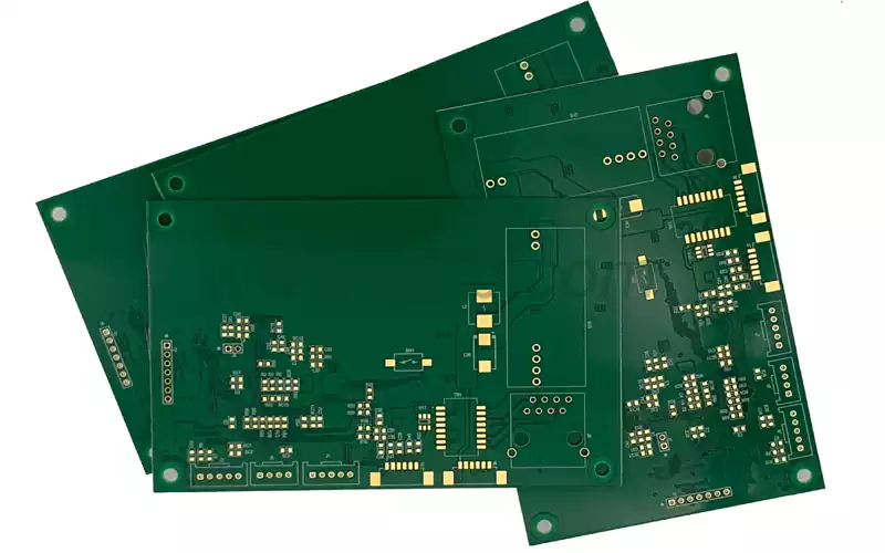
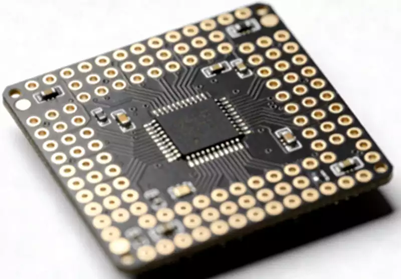
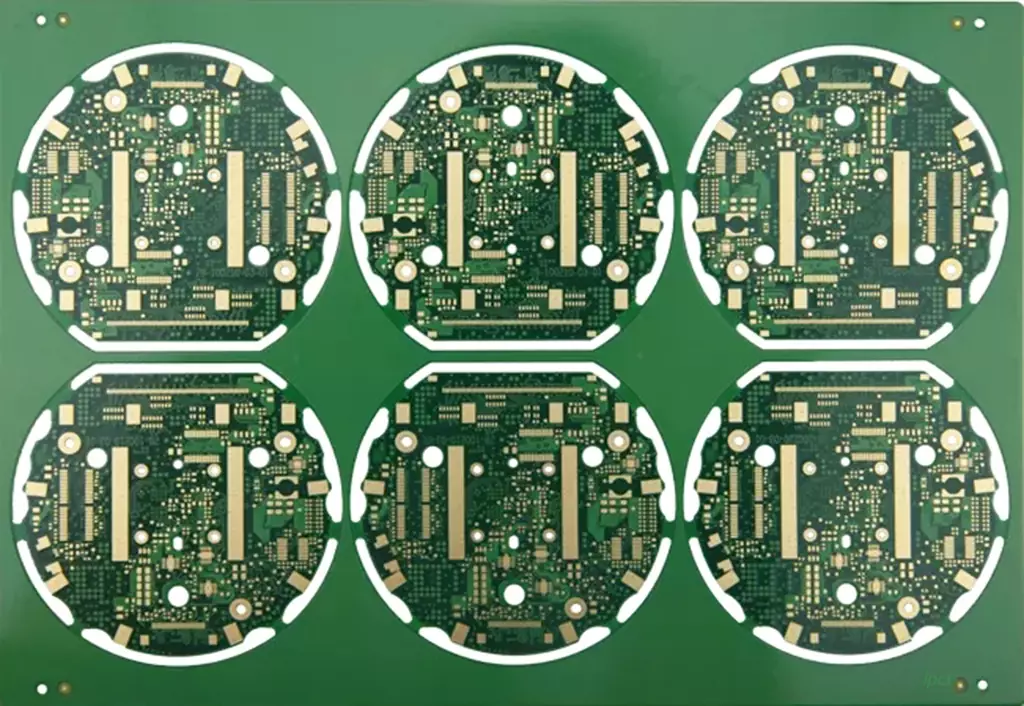
A Power Pole circuit board is a specialized printed circuit board used in power electronics to build and test various switching power-stage circuits. Unlike conventional general-purpose PCBs, a Power Pole board is centered around high-power switching devices and integrates gate-driver circuits, voltage and current sensing circuits, and protection circuitry. It can also support multiple reconfigurable power-conversion topologies, making it suitable for both power electronics education and converter development.
The power pole is one of the fundamental switching building blocks used in power converters. A conventional power pole commonly adopts a half-bridge architecture consisting of two switching devices connected as the main switching leg. Depending on the converter topology, freewheeling or commutation diodes may also be incorporated to provide appropriate current paths and enable efficient power conversion.
A Power Pole circuit board designed for power electronics education and laboratory experimentation integrates the switching core with the associated auxiliary circuits. A typical experimental board includes two power MOSFETs, two power diodes, MOSFET gate-driver circuits, a PWM signal-generation circuit, overvoltage and overcurrent protection circuits, and voltage and current sensing circuits.
The Power Pole circuit board is highly reconfigurable, allowing the same basic power-stage circuit to be used for multiple converter experiments. By replacing the associated magnetic components or connecting different daughterboards, the power stage can be quickly configured for different converter topologies, including buck, boost, buck-boost, flyback, and forward converters.
Key Components of a Power Pole Circuit Board
The power switching devices form the core of the entire circuit board. Power MOSFETs are commonly selected as the primary switching devices because of their fast switching capability and, when properly selected for the application, low conduction losses.
The performance of the gate-driver circuit is equally important to the stability and switching performance of the power stage. The gate-driver IC must provide sufficient gate-drive voltage and peak drive current to charge and discharge the MOSFET gate effectively while maintaining precise timing between the high-side and low-side switching devices. An improperly designed gate-drive layout can result in excessive voltage ringing, increased switching losses, and unstable switching behavior. In severe cases, inadequate timing control can cause both switches in the same half-bridge leg to turn on simultaneously, resulting in shoot-through current and potentially catastrophic damage to the power devices.
Power diodes primarily provide freewheeling current paths and support the required current commutation mechanism for different converter topologies. Key diode parameters, including forward voltage drop, reverse-recovery characteristics, and parasitic capacitance, directly affect converter efficiency, switching noise, and transient response.
The Power Pole circuit board also integrates dedicated voltage and current sensing circuits for monitoring electrical parameters at the input and output. Standardized test points are typically provided to facilitate oscilloscope measurements of switching waveforms and allow engineers or students to analyze the operating conditions of the power converter during experiments.
Protection circuitry is essential for laboratory safety and overall system reliability. On-board overcurrent and overvoltage detection circuits continuously monitor operating conditions and can rapidly initiate protective actions when abnormal conditions are detected, reducing the risk of damage to the power semiconductor devices and the overall converter.
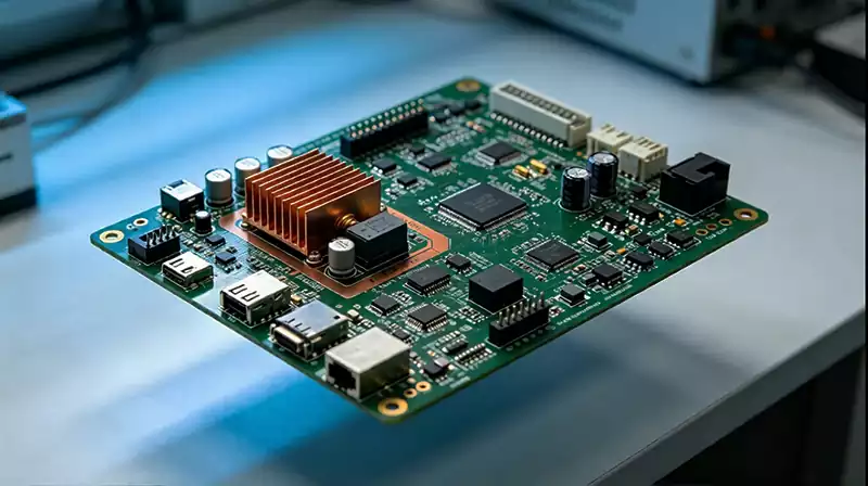
PCB Layout Considerations for Power Pole Circuit Boards
As switching frequency and operating current increase, PCB layout becomes increasingly important to the electrical performance, efficiency, and reliability of a power conversion system.
Switching power stages contain multiple high-di/dt current loops. Although parasitic parameters may not appear in the schematic, actual PCB traces inherently have resistance and parasitic inductance. During high-speed switching transitions, parasitic inductance generates transient voltage overshoot when the current changes rapidly, according to:$$V = L \times \frac{di}{dt}$$
As switching edge rates become faster, even a small amount of stray inductance can produce significant transient voltage spikes, potentially affecting switching stability and increasing device stress.
For this reason, the area of high-frequency, high-current switching loops should be minimized as much as possible. Critical components in the switching path, such as the MOSFETs, input or DC-link capacitors, and diodes, should be placed close together to minimize the physical current loop and reduce the influence of parasitic inductance and resistance.
The gate-drive loop also requires a short, low-impedance current path. Gate-drive traces should have a well-defined and controlled return path. Where the mechanical structure permits, the gate-driver IC should be placed as close as possible to the corresponding MOSFET to minimize trace length and parasitic inductance.
An improperly optimized gate-drive layout can increase electromagnetic interference, switching losses, and voltage ringing while subjecting the power semiconductor devices to excessive electrical stress over long operating periods, ultimately reducing system reliability and service life.
Power Pole circuit board Routing and Copper Design Guidelines
A Power Pole circuit board must handle both continuous steady-state current and high-frequency pulsed switching current. As a result, the PCB must provide adequate current-carrying capacity, low electrical resistance, and effective thermal performance. Copper thickness, trace width, internal power-plane configuration, via arrays, and connector selection all contribute to the maximum current capability and operating stability of the board.
For high-current paths, large-area copper pours or solid copper planes should be preferred over narrow traces whenever the board structure permits. A larger copper cross-sectional area reduces DC resistance and conduction losses while also increasing the available surface area for heat spreading.
Simply increasing copper width, however, does not fully address the design requirements of a high-power PCB. The designer must also consider the actual current distribution, return-current paths, current crowding around vias and pads, and the placement of high-frequency decoupling capacitors. The entire power-current path should be optimized as a complete electrical structure.
In multilayer power electronics PCBs, internal copper planes can be used to establish low-impedance power and return-current paths. When current transitions between PCB layers, multiple parallel vias should be used to reduce vertical interconnect impedance and prevent localized heating and uneven current distribution.
The overall PCB layout should therefore be developed around the actual current paths, rather than treating individual components as isolated placement objects.
Gate-Drive Layout and Switching Performance Optimization
The layout of the gate-drive circuit directly affects mosfet switching characteristics and the dynamic performance of the entire converter. Because a mosfet gate behaves primarily as a capacitive load, the gate-driver must continuously source and sink current to charge and discharge the gate capacitance during switching transitions. Higher switching speeds generally require higher peak gate-drive currents.
The power pole circuit board traces between the gate-driver IC and MOSFET gate should be as short as possible and should provide a clean, low-inductance return path. Uncontrolled parasitic inductance can cause gate-voltage ringing and unwanted oscillation, resulting in unstable switching behavior.
The switching timing of the high-side and low-side devices must also be carefully controlled. If both devices turn on simultaneously, a very large shoot-through current can flow directly through the half-bridge, potentially destroying the power-stage devices.
Therefore, dead time, gate resistance, gate-driver architecture, and PCB parasitic parameters must be designed and optimized as an integrated system rather than treated as independent design variables.
Thermal Management of Power Pole Circuit Boards
Power semiconductor devices generate power losses during operation, which are ultimately dissipated as heat. An effective thermal path is therefore required to transfer heat from the semiconductor junction to the surrounding environment and prevent excessive junction temperatures and thermal failure.
A complete thermal path may include the semiconductor package, PCB copper, thermal vias, internal copper planes, heat-spreading structures, external heat sinks, and ambient airflow.
Many Power Pole laboratory boards use discrete power semiconductor devices combined with dedicated heat sinks. The MOSFETs, diodes, and thermal-management components are concentrated in the power-stage area to maintain adequate heat dissipation under high-power operating conditions.
A customized Power Pole PCB thermal-management strategy should be determined according to device power dissipation, switching frequency, copper area, semiconductor package type, airflow conditions, and enclosure design. Thermal vias can transfer heat from device pads into internal or bottom-layer copper planes, but thermal performance is determined by the overall thermal path and heat-spreading structure. Simply increasing the number of thermal vias does not necessarily result in proportional improvements in thermal performance.
Voltage and Current Sensing Design
High-accuracy voltage and current sensing is fundamental to closed-loop converter control and experimental data acquisition. Depending on the electrical operating conditions and isolation requirements, designers can use different sensing methods, including shunt resistors, Hall-effect current sensors, and current transformers.
The layout of voltage-sensing circuits also requires careful consideration. The sensing network must connect precisely to the intended electrical nodes while being physically separated from high-frequency switching regions whenever possible. This helps prevent switching noise from coupling into the sensing signal and distorting measurement results.
Standard Power Pole laboratory boards typically provide dedicated sensing circuits and measurement terminals so that converter operating parameters can be monitored in real time and switching behavior can be evaluated during experiments.
In high-frequency switching systems, the routing strategy for sensing signals is particularly important. Even when the schematic is electrically correct, an improperly designed PCB layout can introduce common-impedance coupling, parasitic capacitance, and ground noise, resulting in measurement errors and preventing the sensing circuitry from accurately representing the actual operating condition of the converter.
EMI and Signal Integrity Considerations
Because the switching devices on a Power Pole circuit board repeatedly turn on and off at high frequency, rapid changes in voltage and current can generate electromagnetic radiation and electromagnetic interference (EMI).
Major sources of interference include large high-frequency switching loops, excessive voltage slew rates, waveform ringing, poor grounding structures, and uncontrolled current-return paths.
From a PCB design perspective, minimizing the area of high-frequency current loops is one of the most direct and effective methods for reducing EMI. Input or DC-link decoupling capacitors should be placed as close as possible to the switching power stage to minimize the high-frequency current path and prevent long PCB traces from introducing additional parasitic inductance, resistance, and radiated noise.
The power stage and control/sensing circuitry should also be physically separated whenever practical. Sensitive feedback and measurement signals require appropriate isolation from high-current switching nodes to prevent switching noise from coupling into low-level control signals.
For demanding applications, additional techniques such as shielding structures, EMI filters, differential sensing, controlled-impedance routing, and dedicated ground or reference planes can be employed to further improve electromagnetic compatibility (EMC) and signal integrity.
Manufacturing Considerations
The manufacturing requirements for power electronics PCBs differ significantly from those of conventional low-power digital circuit boards. High-current applications often require heavy-copper PCB technology, while large copper areas impose additional challenges on etching, electroplating, soldering, dimensional accuracy, and overall process control.
Large heat-spreading structures and power semiconductor packages can also alter the local thermal distribution of the PCB and affect solder-joint formation during assembly. Therefore, PCB design should simultaneously consider component footprints, thermal interfaces, heat sinks, external connectors, and mechanical mounting structures to ensure compatibility with downstream PCB assembly processes.
Electrical testing is another critical stage in Power Pole PCB manufacturing. The production test sequence may include continuity testing, insulation testing, functional testing, sensing-accuracy verification, gate-drive performance testing, and thermal-performance evaluation.
For laboratory and educational platforms, sufficient standardized test points should be provided to facilitate subsequent measurements of MOSFET drain-source voltage, gate-drive waveforms, switching current, and converter output characteristics.
The Core Value of Power Pole Circuit Board Layout
A Power Pole circuit board is a comprehensive engineering platform that integrates power-stage design, PCB layout, thermal management, control circuitry, and manufacturing technology.
The electrical topology and operating parameters are defined during the power-stage design process. PCB layout determines current paths and parasitic parameters. Thermal design manages semiconductor power dissipation and heat transfer. The control and gate-drive circuits determine switching dynamics, while manufacturing processes ultimately affect product consistency, reliability, and long-term performance.
This integrated design requirement is one of the key differences between power electronics PCB design and conventional digital PCB routing.
A compact and optimized switching loop can significantly reduce the influence of parasitic inductance and resistance. Proper gate-drive routing can improve switching performance and reduce unwanted ringing. A well-designed copper structure can lower conduction losses while improving heat spreading. Robust voltage and current sensing combined with effective protection circuitry can substantially improve the reliability of the entire power conversion system.
A Power Pole circuit board is therefore not only an efficient and flexible platform for power electronics education and laboratory experimentation, but also a representative application that demonstrates many of the fundamental challenges and critical design principles involved in modern power electronics PCB design.