In today’s world of rapidly evolving microelectronic packaging, high-density interconnects, and multilayer board stacking technologies, complex circuit boards with dozens or even hundreds of layers permeate the interiors of high-end servers and supercomputers. However, within the vast global electronics manufacturing industry, there exists a fundamental and historically significant physical carrier that still occupies the core of billions of devices—the single sided PCB design.
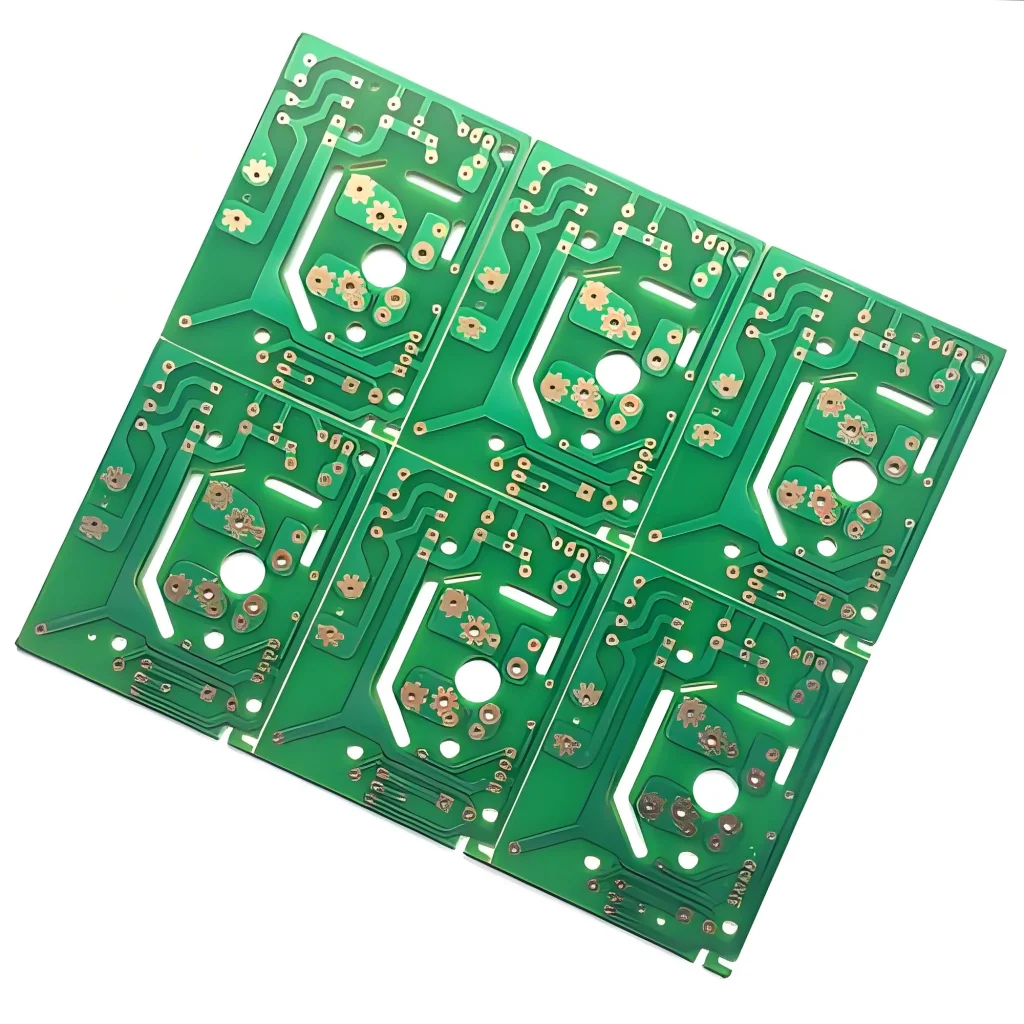
From home appliance control boards, LED lighting drivers, and consumer power adapters to the sensing front-ends of industrial instruments, single-sided PCBs, with their extremely low manufacturing costs, minimal physical topology, and high throughput, form the economic and technological cornerstone of modern large-scale industrial manufacturing.
However, “minimalist structure” does not equate to “simple design.” On the contrary, without the internal ground plane of multilayer boards, without buried or blind vias, and with all metal traces confined to a single two-dimensional physical plane, designing a single-sided PCB is an extreme engineering challenge involving “planar graph theory topology,” “electromagnetic compatibility (EMC) control,” “parasitic parameter compensation,” and “mechanical and thermal stress management.”
The Essence and Material Anatomy of Single-Sided PCBs
To deeply understand the design limitations and advantages of single-sided PCBs, we must first discuss their physical microstructure, material composition, and the limitations of their physical manufacturing processes.
Microscopic Physical Stack-Up Structure
The physical structure of a single-sided PCB can be simplified to four tightly bonded insulating and conductive layers:
Substrate Layer (Base Material)
The insulating substrate forms the physical framework of the entire PCB, providing mechanical strength and electrical insulation. In single-sided PCBs, the most common substrate materials include paper-based phenolic resin composites (such as the well-known FR-1 and FR-2), paper-based epoxy resins (such as FR-3), synthetic fiber glass cloth epoxy resins (FR-4), and aluminum substrates (used for high-power LEDs). Paper-based phenolic materials are extremely low-cost and easily mechanically punched, making them the preferred choice for very low-cost consumer electronics; while aluminum substrates utilize the high thermal conductivity of aluminum to handle high-power heat dissipation.
Copper Foil Layer: Copper foil is a tightly rolled or electroplated conductive metallic layer on one side of a substrate, typically between 18 and 70 micrometers thick. All electrical traces, pads, and junctions are formed by chemically etching this thin layer of copper.
Solder Mask: An insulating protective coating applied to the surface of the copper foil traces, typically green, white, or black. Its main physical function is to prevent the copper foil from oxidizing when exposed to air and to prevent molten solder paste from flowing into padless areas during automated wave soldering, thus preventing bridging and short circuits.
Silkscreen Layer: Marking ink printed on the insulating or solder mask side of the circuit board. It is used to mark component numbers, polarity indicators, warning icons, and test points, guiding manual assembly or automated optical inspection (AOI).
Core Physical Constraints of Single-Sided Topology: Compared to double-sided or multilayer boards, single-sided PCBs face three extremely stringent physical constraints in manufacturing:
Single-sided conductivity limitation. All electrical signal traces, power lines, and ground lines must run on the same two-dimensional plane. If two traces physically intersect, they will connect directly, causing a short circuit.
Non-Plated Through-Hole (NPTH). Drilled or punched holes on a single-sided board serve only as mechanical channels for component leads; the hole walls have no copper plating. This means that component leads must be soldered and electrically connected to the copper foil pads on the bottom, and the through-hole itself cannot be used for signal conduction between layers.
Soldering heat capacity limitations. Due to the single-sided copper foil, the physical peel strength between the pads and the insulating substrate depends entirely on an extremely thin layer of adhesive or a direct heat-pressed interface. During manual soldering or wave soldering, if the pads are heated for too long, the copper foil can easily detach and peel off, causing permanent damage to the board.
Planar Graph Theory and the Engineering Art of Cross-Decoupling
The core challenge of single-sided PCB design lies in transforming a complex logic circuit diagram into a physical topology network on a two-dimensional plane with no trace intersections. Mathematically, this corresponds to the classic “Planar Graph” embedding problem.
Applications of Planar Graph Theory in Routing
In graph theory, if a graph can be drawn on a plane and any two edges have no intersections except at vertices, then this graph is called a planar graph.
A circuit schematic diagram is essentially a non-planar graph. When mapping the pin connection network (netlist) of hundreds of electronic components onto a single layer of copper foil on a single-sided PCB, direct connections inevitably create a large number of intersections.
To untangle these intertwined networks in two-dimensional physical space, engineers must employ topology transformation strategies:
Geometric rotation and spatial reorganization of component layout: By rotating the orientation of chips, transistors, or resistors, networks with numerous interconnects are made to face each other in space, transferring crossing lines to logic connections within the components.
Utilizing physical channels beneath components: Two-pin components such as through-hole resistors, capacitors, and diodes have a physical span between their two pins. Engineers can cleverly route one or more other signal traces through the insulating substrate surface beneath these components, using the “spatial span” of the component body as a physical bridge.
Physical intervention and cost balance of jumper wires: When the topological complexity of the circuit diagram exceeds the computational limits of a purely two-dimensional plane, jumper wires must be introduced to break the two-dimensional constraints.
Jumper wires are typically tin-plated upright or horizontal metal wires (or zero-ohm surface mount resistors) mounted on the non-copper foil side (top layer) of the circuit board, with their two pins passing through substrate holes and soldered to copper foil pads on the bottom layer.
In physical essence, a jumper is a minimalist “second-layer trace.” It achieves physical isolation and crossing of two signal lines through a tiny jump in three-dimensional space.
However, in mass industrial production, the number of jumpers is strictly limited:
Increased assembly costs: Each additional jumper means two more mechanical punching operations, one more jumper insertion operation, and additional material procurement costs.
Restrictions on automated manufacturing: Automated jumper insertion machines require additional processing time; if the number of jumpers is too high, it will significantly reduce the production line’s throughput efficiency.
Therefore, one of the key indicators for evaluating the quality of a single-sided PCB design is whether engineers can reduce the number of jumpers to zero or even single digits while fully ensuring electrical performance.
Electromagnetic Compatibility (EMC) and Signal Integrity in Planar Physics
In multilayer PCB designs, engineers can rely on complete power and ground planes to absorb electromagnetic radiation, provide low-impedance signal return paths, and control characteristic impedance. However, in single-sided PCBs, without a large continuous copper foil as a reference plane, electromagnetic compatibility (EMC) and signal integrity (SI) issues become extremely acute.
Loop Area Minimization and Electromagnetic Radiation Control
According to the laws of electromagnetic induction and antenna theory, a closed current loop radiates electromagnetic waves and is also highly susceptible to external electromagnetic interference (EMI). The intensity of loop radiation is directly proportional to the physical area enclosed by the loop.
In single-sided PCBs, due to the lack of a bottom ground plane, signal lines and their corresponding return current lines (ground lines) are easily separated in the planar routing, forming large physical loops.
To solve this electromagnetic physics problem, single-sided designs must follow the “parallel return current principle”:
Mesh grounding and tracking grounding: The ground line is routed parallel to critical high-frequency signal lines (such as crystal oscillator signals, PWM drive signals, or high-frequency clock signals), ensuring that the signal current and return current are infinitely close in physical space, thus canceling out the generated magnetic fields.
Power and ground topology pairing: Power and ground traces should be run parallel and closely spaced on a plane, like twisted-pair cables, forming a “star” or “tree” distributed power supply topology. DC ground loops with breaks should be avoided.
Parasitic inductance, parasitic capacitance, and common impedance coupling:
Because single-sided PCB traces are typically longer and wider than microstrip lines on multilayer boards and lack ground plane shielding, the parasitic inductance and capacitance effects of the traces themselves are particularly significant.
When high-frequency transient currents (such as the switching on and off of a switching power supply transistor) flow through a single-sided ground trace with parasitic inductance, a non-negligible voltage drop occurs on the ground trace; this phenomenon is called “ground bounce.”
In single-sided PCBs, because all circuits share a single-plane branched ground trace, the ground bounce voltage of a high-power device (such as a relay or power amplifier transistor) can directly couple into sensitive microcontroller or analog sensor circuits, causing severe common impedance coupling interference.
The planar topology strategy for solving this problem is “Single-Point Grounding”: The grounding network of the entire circuit board is divided into “High Voltage/Power Ground,” “Low Voltage/Digital Ground,” and “Sensitive/Analog Ground.” These three grounding paths are completely independent on the plane, do not intersect, and only physically converge at a single point at the negative terminals of the capacitors at the power input. This single-point convergence topology physically cuts off the propagation path of common impedance coupling.
Thermodynamic Management and Thermal Design of Power Single-Sided PCBs
Single-sided PCBs are widely used in switching power supplies, LED lighting, home appliance drives, and other fields containing high-power devices. These devices generate significant heat accumulation during operation. Because a single-sided PCB has only one layer of copper foil, its thermal conductivity and heat dissipation capabilities are severely limited.
Copper-Clad Thermal Dissipation and Thick Copper Processes
In ordinary single-sided circuit boards, heat is mainly radiated to the surrounding air through the copper foil surface and conducted to the back side through the insulating substrate. However, paper-based or epoxy resin substrates are themselves poor conductors of heat, with extremely low thermal conductivity.
To improve planar heat dissipation efficiency, engineers lay large areas of “thermal copper powder” around the pads of high-power devices (such as MOSFETs, rectifier bridges, and high-power resistors).
According to the physical laws of thermal conduction, heat diffuses much faster inside the copper powder than through the substrate. The large copper powder quickly flattens and expands point heat sources concentrated on the tiny chip package into a large area heat source, which is then dissipated through convection into the air via the solder mask.
In high-power single-sided power supply designs, factories also employ “heavy copper technology,” increasing the default 35-micron copper foil thickness to 70 microns, 105 microns, or even 210 microns. Thicker copper not only can withstand currents of tens of amperes but also significantly reduces thermal resistance, enhancing planar heat dissipation capabilities.
Engineering Physics of Aluminum-Backed PCBs
When power density exceeds the thermal conductivity limits of traditional FR-4 insulating substrates (e.g., in 100-watt LED arrays), aluminum-backed PCBs become the only option.
The microscopic topology of aluminum-backed PCBs is extremely unique:
The bottom layer is a single piece of aluminum plate with high thermal conductivity and high mechanical strength.
On top of the aluminum plate is an extremely thin (typically only tens of micrometers thick) layer of a special high-thermal-conductivity insulating polymer dielectric layer with extremely high dielectric strength.
The top layer is a single layer of copper foil used for etching wiring.
In aluminum-backed PCBs, high-power devices are soldered onto the top copper foil. The heat generated by the devices is instantly conducted through the thin, high-thermal-conductivity insulating dielectric layer to the thick aluminum plate at the bottom, and then connected to an external heatsink via the aluminum plate. Aluminum-backed PCBs perfectly unify the seemingly conflicting physical properties of insulation and thermal conductivity within a single-layer topology.
DFM (Design for Manufacturing) and Automated Production Practices of Single-Sided PCBs
The core commercial advantage of single-sided PCBs lies in “extreme cost control and ultra-high output efficiency.” Whether this advantage can be realized depends 90% on whether the designer has achieved excellence in DFM.
Mechanical Punching Process and Hole Diameter Design Specifications
For insulating single-sided boards using FR-1 or FR-2 paper-based materials, industrial production typically does not use expensive and slow CNC drills, but instead employs “high-speed die mechanical punching.”
The punching die uses tremendous physical impact force to punch hundreds of through-holes on the entire PCB in a single instant. This process imposes special geometric constraints on single-sided PCB design:
Hole Diameter to Board Thickness Ratio Limitation: The minimum hole diameter must not be less than the physical thickness of the board material. If the hole diameter is too small, the punch pins are easily bent or broken under the enormous impact force.
Hole Edge Distance and Edge Safety Distance: The physical distance between the hole edge and the board edge, as well as between holes, must be greater than a set threshold. If the distance is too close, the paper-based material will crack or delaminate under the stress of punching crack propagation.
Annular Ring Width Compensation: Because the positioning accuracy and die wear tolerance of mechanical punching are significantly greater than those of precision CNC drilling, the copper foil pads on the single-sided board must be designed to be large enough, with a very generous annular width. Otherwise, if the punching is misaligned, it will directly knock off or break the copper foil pads on the single-sided board, resulting in an open circuit and scrap.
Wave Soldering: Physics and Anti-Bridging
After component insertion, most single-sided PCBs are soldered in large batches using automated wave soldering machines.
During wave soldering, the bottom of the entire PCB smoothly passes through a wave of pumped-up molten solder. Because single-sided boards lack the capillary action of metallized vias (capillary action cannot draw molten solder into the vias), soldering relies entirely on the wettability of the bottom conductive pads and the component leads.
This physical process is highly susceptible to two manufacturing defects:
Bridging: When two closely spaced traces or pads simultaneously leave the molten solder wave, surface tension causes a molten metal bridge to form between them, resulting in an absolute short circuit.
Cold Solder/Tombstoning: Due to a mismatch in pad thermal capacity, the leads fail to reach the molten solder temperature, preventing the molten solder from wetting the leads.
To completely eliminate wave soldering defects at the design level, single-sided PCBs must employ specialized pad geometry topologies:
Teardrops and Solder Snipes: Teardrop-shaped transition copper foil is added at the junctions of all traces entering the pads to prevent mechanical stress breakage. Simultaneously, at the ends of densely packed IC pins, specially designed “induced anti-bridging pads” that are not connected to any electrical network are used. These pads utilize liquid surface tension to drag excess molten solder onto the induced pads, ensuring the absolute independence of the main pins.
Directional Layout Strategy: The routing of all rectangular pads and IC traces on the entire PCB must be parallel to the physical direction of the conveyor belt as the PCB passes through the wave soldering machine. Pads aligned with the solder wave flow direction can smoothly detach from the molten solder, while pads perpendicular to the flow direction are highly susceptible to intercepting the solder flow and creating short circuits.
Conclusion: The Engineering Wisdom Behind Minimalist Physics
Single-Sided PCBs may seem like the most primitive and simplest member of the PCB family, but they vividly illustrate the core philosophy of industrial engineering: “creating ultimate value under extreme constraints.”
In the two-dimensional physical world without multi-layer stacking or metallized via reference planes, single-sided PCB designers must integrate graph theory topology, electromagnetic boundary conditions, thermal conductivity, and mechanical stress. Every jumper placement, every ground wire laying, and every pad’s stretching represents a precise balance between material physical properties and cost control.
Whether laying the foundation for the electronics industry over the past decades or leading the modern wave of green, low-carbon, and cost-effective mass manufacturing, single-sided PCBs continue to shine with unique engineering wisdom in the vast sea of industrial manufacturing, thanks to their irreplaceable economic and physical characteristics.