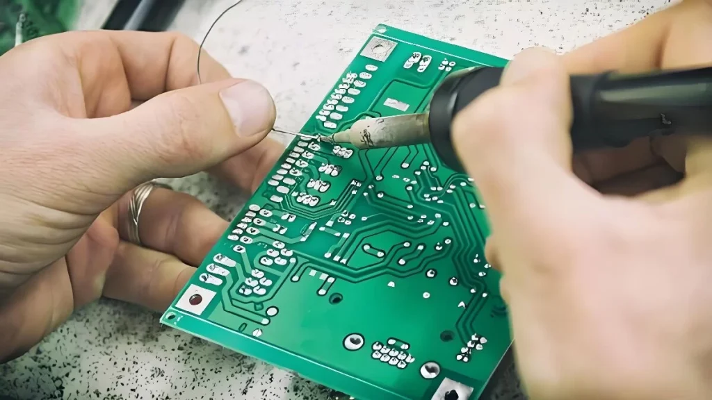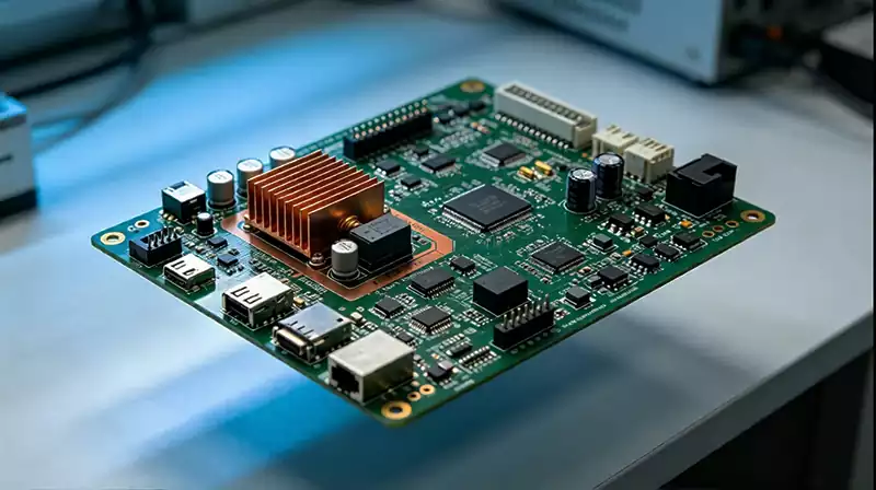
Developing a new electronic product often requires several rounds of circuit board testing before the design is ready for production. A low cost pcb prototype helps engineers evaluate circuit functionality, identify layout problems, and verify component compatibility without committing to a large manufacturing run. However, reducing the initial price is only part of the goal. A useful prototype must also provide reliable test results and support the next stage of product development.
The cost of a pcb prototype depends on more than the number of circuit boards ordered. Layer count, board dimensions, material specifications, drilling requirements, copper features, surface finish, and delivery time all influence fabrication expenses. If components are assembled onto the pcb boards, component sourcing, placement complexity, soldering, and testing add further costs.
The most effective approach is to simplify what does not contribute to performance while preserving the electrical and mechanical requirements that make the prototype meaningful.
What Determines the Cost of a PCB Prototype?
The first step toward a more affordable prototype is understanding which design decisions increase manufacturing cost. Some factors are easy to change early in development, while others are essential to the product’s intended function.
Layer count is one of the most important considerations. A simple two-layer board is generally less expensive to fabricate than a four-layer or six-layer design because additional layers require more material, lamination, drilling, and processing. If the circuit can meet its routing, grounding, and signal-integrity requirements with fewer layers, a simpler stackup may reduce the prototype budget.
Nevertheless, removing layers is not always economical. High-speed digital circuits, compact wireless devices, and designs with demanding electromagnetic compatibility requirements may need additional reference planes or routing layers. Reducing the layer count without evaluating these requirements can create interference problems, increase routing difficulty, or lead to another prototype revision.
Board size also affects cost. Larger outlines consume more panel area, while irregular shapes and extensive cutouts can reduce panel utilization. Reviewing the board dimensions and component placement together may reveal opportunities to use space more efficiently. For a low cost pcb prototype, compactness should be balanced against assembly access, thermal performance, connector placement, and mechanical clearance.
Material and fabrication specifications also influence the quotation. Standard FR-4 is suitable for many general-purpose electronic designs, but applications requiring specialized dielectric properties, higher thermal performance, or controlled electrical characteristics may need different materials. Similarly, fine trace widths, tight spacing, small drill diameters, blind or buried vias, and specialized surface finishes can introduce additional processing requirements.
The right target is not the lowest possible specification. It is the simplest specification that reliably satisfies the circuit’s actual requirements.
Design Choices That Reduce Fabrication Expenses
Cost optimization is most effective before the PCB layout is finalized. Once a design has been routed and prepared for manufacturing, changing its construction can require substantial engineering work.
Start by reviewing whether every layer, via structure, and fine-pitch feature is necessary. Through-hole vias may be a practical choice when space permits and the design does not require the routing density offered by blind or buried vias. Standard drill sizes and manufacturable trace widths can also help avoid unnecessarily demanding fabrication processes.
Component placement deserves similar attention. Connectors, large components, mounting holes, and test points should be arranged to support both the intended circuit and the manufacturing process. Adequate spacing can simplify assembly and inspection, while accessible test points can make debugging more efficient. Eliminating unnecessary features is useful, but removing test access that engineers need to diagnose faults may make later revisions more expensive.
Material selection should follow electrical and environmental requirements rather than price alone. If the prototype operates within the capabilities of standard FR-4, there may be no reason to select a more expensive high-frequency laminate. If the circuit depends on low dielectric loss or tightly controlled impedance, however, substituting a cheaper material without validating its performance can produce misleading test results.
Surface finish is another decision worth reviewing. Different finishes offer different solderability, shelf-life, contact, and assembly characteristics. The least expensive option is not automatically appropriate for fine-pitch components, repeated assembly cycles, or specific contact requirements. Choose a finish that supports the intended process and component interfaces.
For a low cost pcb prototype, design-for-manufacturing review should happen before fabrication data is released. Checking minimum features, clearances, drill requirements, stackup details, and component footprints can help prevent avoidable manufacturing questions and costly redesigns.
Choose the Right PCB Prototype Quantity and Delivery Schedule
Ordering only a few circuit boards may seem like the cheapest option, but the total quotation does not always increase in direct proportion to quantity. Manufacturing preparation, engineering review, and other setup activities can contribute fixed costs to a small order. Producing a few additional boards may therefore provide useful spares or support parallel testing for a relatively modest increase in total cost.
The best quantity depends on how the prototype will be used. A single engineering sample may be sufficient for checking basic dimensions or an early circuit concept. Several boards may be more appropriate when different firmware versions, component alternatives, or environmental tests need to be evaluated at the same time.
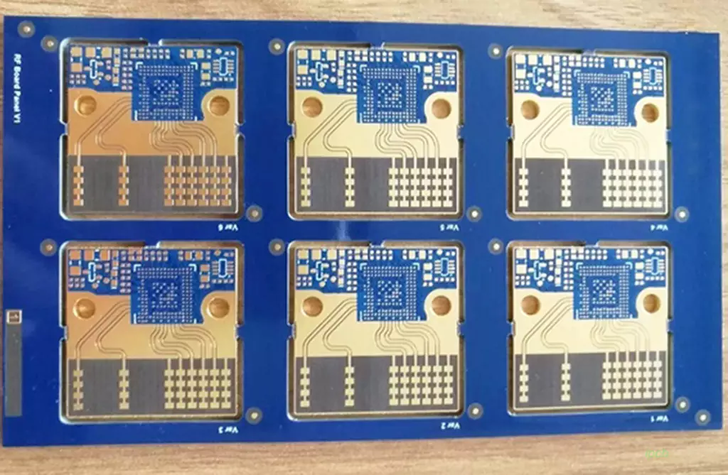
Panelization can also affect the economics of small orders. When the board dimensions and manufacturing specifications fit a shared production panel, the manufacturer may be able to distribute panel-processing costs across multiple designs. Whether this option is available depends on the fabrication process and order requirements, so it should be confirmed during quotation rather than assumed.
Delivery time is another important variable. Expedited fabrication can increase costs because production must accommodate tighter scheduling and material availability constraints. Planning prototype orders around the development schedule can reduce the need for rush processing.
A low cost pcb prototype should arrive when the engineering team is ready to test it. Ordering too early may leave boards waiting while the design changes, whereas ordering too late can delay the next development milestone. Coordinating fabrication with component procurement, firmware readiness, and test preparation helps avoid wasted time and unnecessary repeat orders.
Why PCB Prototype Testing Can Save Money Later
A prototype is valuable because it provides evidence about whether the design works as intended. Its purpose is not simply to produce an inexpensive physical board; it is to reduce uncertainty before larger investments are made.
Initial testing may focus on power-up behavior, voltage levels, current consumption, clock operation, communication interfaces, and basic circuit functionality. Depending on the application, engineers may also need to evaluate thermal behavior, signal integrity, electromagnetic interference, or performance under changing operating conditions.
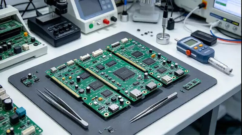
The appropriate test method depends on the design. Visual inspection can reveal obvious assembly issues, while electrical continuity checks help identify certain connection problems. More complex assemblies may require automated optical inspection, X-ray inspection for hidden solder joints, in-circuit testing, or functional testing. Bare-board electrical testing and assembled-board functional testing address different potential failures, so they should not be treated as interchangeable.
Testing should also reflect the prototype’s development stage. An early proof-of-concept board may need only enough verification to establish whether the central circuit idea is viable. A design approaching production usually requires more comprehensive checks of electrical performance, mechanical fit, assembly consistency, and applicable environmental requirements.
The results should guide the next revision. If a board fails because of an incorrect footprint, unstable power distribution, poor grounding, or an unsuitable component, correcting the underlying problem is more valuable than simply ordering another inexpensive batch.
This is why the lowest initial quotation does not always produce the lowest development cost. A slightly more expensive prototype that uses the correct materials, provides useful test access, and meets the intended electrical requirements can prevent repeated fabrication and assembly cycles.
Preparing Files for an Accurate PCB Prototype Quote
A clear manufacturing package helps the supplier evaluate the design and identify requirements that could affect cost or delivery. Missing or inconsistent information may lead to clarification requests, quotation revisions, or delays after an order has been placed.
For bare-board fabrication, prepare the Gerber or ODB++ manufacturing data, NC drill files, board outline, layer stackup, material requirements, copper specifications, surface finish, and any controlled-impedance requirements. Include relevant tolerances and special fabrication instructions where needed.
If the project requires assembly, provide a bill of materials, component placement data, assembly drawings, and instructions for programming or testing. Clarify whether components will be supplied by the customer or sourced by the manufacturer. Component availability, package type, and sourcing restrictions can affect both the schedule and the total assembled-board cost.
The quotation should also distinguish the required services. Bare PCB fabrication, component procurement, SMT assembly, through-hole soldering, inspection, functional testing, and shipping may be priced separately or combined into a turnkey package. Understanding what is included makes it easier to compare quotations on a consistent basis.
For an affordable low cost pcb prototype, accurate documentation and a clear scope of work are practical cost-control tools. They reduce uncertainty before production begins and help ensure that the delivered boards match the intended design.
A successful pcb prototype strategy balances fabrication cost, engineering time, and the value of the test results. By selecting appropriate materials, avoiding unnecessary manufacturing complexity, planning order quantities, and validating critical functions early, engineers can develop a low cost pcb prototype that supports informed design decisions and creates a more reliable path toward production.