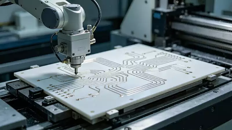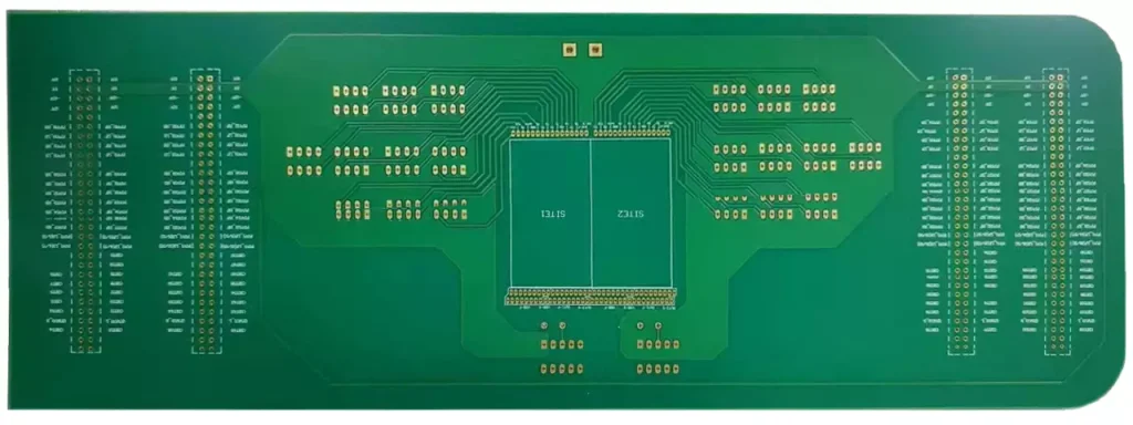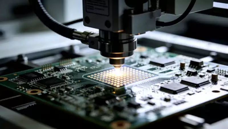
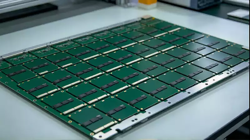
A panel circuit board is a manufacturing arrangement in which multiple individual printed circuit boards are combined into a larger panel for fabrication or assembly. Instead of handling each small PCB separately, manufacturers can process several boards together through production equipment. This approach improves handling efficiency, supports automated assembly, and can reduce production time for suitable designs.
PCB panelization is particularly useful for small boards, irregularly shaped circuits, and products manufactured in repeated quantities. The panel layout must provide enough mechanical support for production while allowing individual boards to be separated without damaging components, copper traces, or board edges.
Why PCB Panelization Matters in Production
Individual PCBs can be difficult to handle when they are small, narrow, or have irregular outlines. During automated assembly, boards need to move through printing, component placement, soldering, and inspection equipment in a stable and consistent manner. Combining multiple boards into a panel creates a larger handling unit that is easier to transport through these processes.
A panel circuit board can also improve production efficiency by allowing several units to be processed in one operation. For example, solder paste printing and SMT placement can be performed across multiple boards within the same panel. This reduces the need to load and position each individual PCB separately.
Panelization can also improve material utilization. By arranging multiple board outlines on a shared panel, manufacturers can use available material more efficiently. The actual benefit depends on board dimensions, spacing, routing requirements, and the manufacturing panel size.
Another consideration is mechanical protection. Some PCBs have components positioned close to their edges, making them vulnerable to impact or handling damage. Adding support rails around the panel can provide additional stability during automated production.
However, panelization is not automatically beneficial for every design. Large boards may already meet equipment handling requirements, while some sensitive or unusually shaped products may require specialized panel arrangements. The decision should account for board geometry, assembly process, production quantity, and separation requirements.
Common PCB Panel Connection Methods
The way individual boards are connected within a panel determines how they are supported during production and how they can be separated afterward. Three common methods are V-scoring, tab routing, and punched connections.
V-scoring creates continuous V-shaped grooves along the boundary between adjacent boards. Only part of the PCB thickness is removed, leaving a thin material section that holds the boards together. After assembly, the individual units can be separated along the scored lines.
This method is generally suitable for rectangular or straight-edged boards arranged in regular patterns. It can provide relatively narrow spacing between adjacent units and make efficient use of panel material. However, the remaining material must be strong enough to support the panel during production. Components that extend beyond the board edge may also interfere with the scoring line or separation process.
Tab routing uses routed gaps to separate individual boards while leaving small connecting tabs between them. These tabs maintain the panel structure during manufacturing and assembly. Small perforations, often called mouse bites, may be added to make separation easier.
Tab routing is more flexible for irregular board shapes and layouts that cannot use continuous straight scoring lines. It can also support designs with curved edges. However, the remaining tabs may leave small protrusions or rough edges after separation, so their positions should be planned carefully.
Punching uses dedicated tooling to create separation features or remove individual boards from a panel. It can be suitable for products requiring repeated shapes and consistent separation, particularly when production volumes justify the tooling investment. The tooling design and mechanical stress during separation need to be considered before selecting this method.
The appropriate connection method depends on board geometry, component placement, edge requirements, production volume, and the capabilities of the manufacturing process.
Important Design Requirements for a Panel Circuit Board
A well-designed panel circuit board must remain mechanically stable throughout fabrication and assembly. The panel should also provide sufficient access for automated equipment and allow reliable separation after processing.
Panel rails are commonly added along the outer edges to provide support and handling space. Their dimensions should be coordinated with the production equipment rather than selected arbitrarily. Wider rails can improve stability but may increase material consumption, so the design needs to balance mechanical support and panel utilization.
Tooling holes help align and secure the panel during manufacturing. Their positions should be consistent with the requirements of the assembly equipment and should not interfere with individual PCB circuits. Fiducial marks are also important because automated optical systems use them as reference points to recognize panel position and correct alignment during solder paste printing and component placement.
The spacing between individual boards must account for the selected separation method and component clearance. Components placed too close to V-score lines or tab connections may be damaged during depaneling. Particular attention should be given to connectors, tall components, and parts with leads or bodies extending beyond the PCB outline.
Electrical and thermal considerations should not be overlooked. Panelization must not introduce unwanted electrical connections between separate circuits. If multiple designs are combined into one panel, their electrical isolation and manufacturing requirements should be clearly defined.
For boards with controlled impedance, high-speed signals, or sensitive RF circuits, the panel arrangement should preserve the electrical design of each individual PCB. The panel structure should also avoid unnecessary mechanical stress on areas containing delicate components or critical connections.
Depaneling and Quality Control
After PCB fabrication and assembly, the individual boards must be separated from the panel. This process is known as depaneling. The separation method should match the connection structure selected during panel design.
V-scored panels can be separated using suitable manual or mechanical equipment. Tab-routed panels may require a depaneling router or other controlled separation equipment. For higher-volume production, automated depaneling systems can improve consistency and reduce manual handling.
Mechanical stress is a major consideration during separation. Excessive force can cause board-edge damage, solder joint cracks, component displacement, or stress-related defects. This is particularly important for boards with brittle components, ceramic packages, or components positioned close to the separation line.
Quality inspection should cover both the assembled boards and the separated edges. Engineers may check for cracks, burrs, damaged solder mask, copper exposure, and other abnormalities. For sensitive products, additional inspection may be needed to confirm that the separation process has not affected electrical performance.
The manufacturing documentation should clearly identify the panel dimensions, individual PCB outlines, connection method, tooling holes, fiducial locations, and separation requirements. Providing these details early helps the manufacturer evaluate the panel design and recommend adjustments before production begins.
A properly planned panel circuit board improves the way individual PCBs move through manufacturing and assembly. By selecting a suitable connection method, maintaining adequate mechanical support, and controlling depaneling stress, engineers can make production more efficient while protecting the quality of each finished board.