In today’s electronics industry landscape, characterized by dozens of layers of high-density interconnects, micron-level linewidths and spacing, and gigahertz-level high-speed signals, single sided PCB boards are often considered the most primitive and fundamental element of electronics manufacturing. However, to underestimate their engineering value and industrial importance is akin to focusing on the glass curtain walls of skyscrapers while ignoring the underground pipe networks and foundations that support the entire city’s infrastructure.
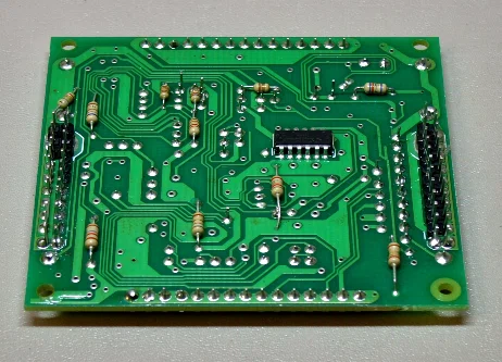
From power control boards, lighting driver modules, remote controls, and sensor interfaces in everyday household appliances to headlight controls, wiper drives, and auxiliary power units in automotive electronics, single-sided PCBs still hold an irreplaceable share in the vast global electronics manufacturing system. With its streamlined, single-conductive-layer architecture, it exemplifies the engineering wisdom of “pursuing ultimate cost efficiency and manufacturing reliability within physical boundaries.”
The Physical Essence and Structural Characteristics of a Single-Sided Conductive Plane
To understand the unique appeal of single-sided printed circuit boards (PCBs), we must first return to their most fundamental physical form: the entire PCB has conductive metal patterns (usually electrolytic copper foil) on only one side, while the other side is a pure insulating substrate surface, typically used to support electronic components or for silkscreen markings.
In the early days of electronic assembly, engineers relied on manual point-and-wire bonding or terminal blocks to connect resistors, capacitors, transistors, and vacuum tubes. This method was not only inefficient and inconsistent, but also prone to loosening and short circuits, making it unsuitable for large-scale industrial production. The advent of single-sided PCBs, for the first time, solidified the previously chaotic three-dimensional flying wires into two-dimensional planar copper foil traces printed on the surface of an insulating substrate. This not only made circuit connections highly standardized and reproducible, but also combined the mechanical fixation and electrical connection of component pins into one.
Compared to double-sided and multilayer boards, single-sided PCBs have three distinct physical architectural characteristics:
First, there are no complex interlayer metallized vias (PTHs). Because it has only a single conductive layer, signals and current do not need to cross the insulating dielectric layer to reach the other side, thus eliminating high-cost and complex processes such as copper plating, hole wall plating, and multi-layer alignment.
Second, the routing topology is strictly limited to a single plane. All conductive paths, pads, and power loops must be laid on the same plane. If two traces meet on the plane, they must avoid each other by detouring, using jumpers, or utilizing the component’s own pin/body structure; otherwise, a short circuit will occur.
Third, the manufacturing process is highly streamlined, resulting in a significant cost advantage. There are no lamination alignment errors, no blind or buried via laser drilling, and no expensive multi-layer prepreg consumption, making single-sided printed circuit boards highly economically competitive in small to medium-complexity circuits and high-volume cost-reduction scenarios.
The Engineering Wisdom of Two-Dimensional Planar Topology and Trace Avoidance
Many people mistakenly believe that “only one copper layer” means a simple design. On the contrary, in circuits with limited space and a large number of components, the two-dimensional planar routing of single-sided printed circuit boards (PCBs) is often an intellectual game testing spatial imagination and topology planning abilities.
Solving Planar Crossovers
The most common challenge in single-sided PCB design is “trace crossing.” When a power line or signal line needs to pass over another trace, since there is no second copper layer to use as a buffer, engineers typically employ several classic methods:
One is clever detours. By adjusting the position of components, rotating the package orientation, or changing the pin assignment, the paths that would otherwise cross become smooth and parallel, eliminating the crossing conflict at its source.
The second is using through-hole components to cross over. In many single-sided through-hole boards, an axial resistor, diode, or jumper can span over the copper foil trace below, using the component’s own physical height and the pads at both ends to achieve a “three-dimensional crossing” without touching the conductive copper wire below.
The third is local zero-ohm resistors or jumper wires for bridging. At critical nodes where space constraints necessitate their placement, a zero-ohm surface-mount resistor or metal jumper can ensure electrical continuity and facilitate subsequent production and testing.
Power and Ground Plane Planning
On single-sided printed circuit boards (PCBs), the lack of independent inner ground or power planes makes the planning of high-current paths and reference ground paths particularly crucial. Engineers typically widen main power and ground traces as much as possible, and when necessary, use large-area copper pours to reduce line resistance and voltage drop.
However, large-area copper pours on single-sided boards require extreme caution. Firstly, large copper areas absorb significant heat during wave soldering or manual soldering (the so-called “heat sink effect”), leading to slow heating of connected pads, poor solder wetting, and even cold solder joints. Secondly, irregular, isolated copper islands or elongated copper tongues can act as miniature antennas under high-frequency interference, causing unnecessary electromagnetic coupling. Therefore, reasonable copper pour boundaries, appropriate heat dissipation ribs, and clear return current path planning are the watershed for the stable operation of single-sided board designs.
The Choice of Insulating Substrate and the Material Science Game
The performance ceiling of single-sided printed circuit boards (PCBs) is largely determined by their insulating substrate. While single-sided boards generally have less stringent requirements for high-frequency, high-speed dielectric properties than multilayer boards, there are still ample material science choices to consider in terms of mechanical strength, heat resistance, flame retardancy, and manufacturing cost.
Paper-based Phenolic Laminates (e.g., FR-1, FR-2, XPC)
Paper-based phenolic resin boards have long played a dominant role in low-cost consumer electronics, toys, remote controls, some small appliances, and basic power modules. This type of substrate uses wood fiber paper as reinforcement, impregnated with phenolic resin, and then hot-pressed.
Its core advantages are low price and extremely high die-cutting efficiency, making it ideal for mass-produced, low-cost standardized products. However, its disadvantages are equally apparent: relatively high hygroscopicity, leading to decreased insulation resistance and mechanical strength in humid environments; and lower heat resistance and bending resistance compared to fiberglass cloth substrates, making it more prone to deformation or delamination under high-temperature welding or frequent mechanical stress.
Composite Substrates (e.g., CEM-1, CEM-3)
To compensate for the shortcomings of paper-based phenolic boards without directly jumping to the more expensive pure glass fiber cloth multilayer system, the electronics manufacturing industry has developed composite substrates. Typical examples include CEM-1 and CEM-3.
These materials typically employ a composite structure of “outer glass fiber cloth + core pulp or special filler.” While maintaining good machinability and moderate cost, they improve dimensional stability and electrical insulation performance, finding wide application in lighting drivers, home appliance control boards, and mid-range industrial auxiliary circuits.
Epoxy Glass Fiber Cloth Substrate (FR-4)
FR-4 remains a reliable choice when single-sided printed circuit boards need to be used in more demanding operating environments, require higher heat resistance, better moisture resistance, or have more robust mechanical structures. FR-4, with alkali-free fiberglass cloth as the reinforcing skeleton and epoxy resin as the matrix, possesses excellent mechanical strength, low water absorption, good flame retardancy, and stable insulation properties, enabling it to withstand the high temperatures of lead-free soldering and a wide temperature range.
The entire manufacturing process from copper-clad laminate to finished circuit board.
Transforming a single-sided printed circuit board from a design drawing into a physical entity requires a series of precise physical and chemical processing steps. Although multi-layer lamination and hole wall electroplating are eliminated, fluctuations in process parameters at each step directly affect the final yield.
Material Cutting and Surface Pretreatment: Manufacturing begins by cutting large sheets of copper-clad laminate into work boards suitable for production line flow according to the production panel dimensions. The pretreatment stage then involves mechanical brushing or chemical micro-etching to clean the copper surface, removing the surface oxide layer, oil, and impurities to ensure that subsequent photosensitive dry or wet films can adhere evenly and firmly to the copper foil surface.
Pattern Transfer and Chemical Etching
A photosensitive resist layer (dry film or liquid photosensitive ink) is applied to the pre-treated copper surface. The circuit pattern is then transferred onto the resist layer using an exposure device. After development, the resist layer in areas that do not require protection is washed away, exposing excess bare copper.
The etching process then begins. An acidic or alkaline etching solution dissolves the exposed copper foil under spray pressure, leaving only the conductive lines and pads protected by the resist layer. After etching, the resist layer is removed, revealing a clear, single-plane copper foil circuit on the substrate. This step requires strict control of the etching rate and lateral etching amount to prevent excessive etching that thins or breaks the fine lines, and to avoid micro-short circuits caused by residual copper between lines.
Drilling or Punching
For through-hole components or mechanical mounting holes, single-sided boards can be drilled one hole at a time using a CNC drilling machine, or high-speed punching and shaping can be performed using specialized dies in mass production. Punching is highly efficient, making it ideal for high-volume, regular-hole-position single-sided board manufacturing; while CNC drilling demonstrates exceptional flexibility in prototyping, multi-variety, small-batch production, and scenarios with frequent hole position changes.
Solder Mask, Surface Treatment, and Silkscreen Printing
To prevent solder bridging and short circuits between adjacent pads during soldering, and to protect the copper foil in non-soldered areas from oxidation, moisture, and contamination, the circuit board surface is coated with solder mask ink (commonly green, but black, white, and blue are also available; for example, high-reflectivity white solder mask ink is often used in LED lighting boards to improve luminous efficiency).
Exposed pads require appropriate surface treatment to ensure good solderability and shelf life. Common solutions include hot air leveling (HASL, lead-containing or lead-free), organic solderability protectant (OSP), and chemical nickel immersion gold (ENIG). Finally, component reference numbers, polarity markings, and border markings are printed on the board surface using silkscreen or inkjet printing processes for easy assembly and maintenance.
Thermodynamics, Electromagnetic Compatibility, and Reliability Engineering
Even though the circuit logic of a single-sided printed circuit board (PCB) may seem simple, it must still adhere to the fundamental laws of the physical world during actual operation. Ignoring thermodynamic and electromagnetic compatibility boundaries often leads to early, unreproducible failures in the field.
Heat-generating Devices and Thermal Fatigue Control
In single-sided PCBs used for power conversion, motor drives, or LED lighting, power devices (such as power MOSFETs, rectifier bridges, high-power resistors, and constant-current drive chips) are often the primary heat sources. If heat is concentrated in a small, localized area and cannot dissipate, it will not only cause increased junction temperatures and shorten device lifespan but also create localized thermal expansion stress in the substrate, potentially leading to solder joint fatigue cracking or pad lifting under long-term cycling.
Therefore, during the single-sided PCB design phase, high-heat-generating components should be reasonably distributed to avoid clustering. If necessary, extend the heat dissipation copper foil around the pads, add heat sinks, or select a substrate with better thermal conductivity (such as metal-based PCBs, which are often used as an extension of single-sided thermal design in ultra-high heat flux density lighting and power scenarios).
Electromagnetic Radiation and Interference Immunity Considerations
Single-sided printed circuit boards (PCBs) lack a complete multi-layered reference ground plane, making them more prone to forming large current loops when facing high-frequency switching signals or inductive load switching. The larger the current loop area, the stronger the ability to radiate electromagnetic interference (EMI), and the easier it is to pick up external electromagnetic noise.
In design, reducing the area of high-frequency switching loops, routing signal lines close to their corresponding ground lines, and properly placing filter capacitors and ferrite beads at power inputs are key measures to control the electromagnetic compatibility (EMC) performance of single-sided PCBs. For noise-sensitive analog sampling or communication interfaces, sensitive traces should be kept away from strong interference sources and high-current paths.
Assembly Process and Structural Stress Protection
During subsequent wave soldering, reflow soldering, or manual soldering, the PCB will experience rapid temperature rises and falls. If the single-sided PCB has an unreasonable panelization design or is too thin, localized bending stress can easily occur during transfer, depaneling (V-cut or perforated board splitting), and casing screw tightening. Brittle components such as ceramic capacitors, if placed close to the board edge or partition line, are highly susceptible to micro-cracks under partitioning or assembly stress, posing a potential reliability hazard.
In the era of intelligent and green manufacturing, value is being reshaped.
Some may ask: with the widespread adoption of high-density interconnect (HDI), rigid-flex boards, and advanced packaging technologies, will single-sided printed circuit boards (PCBs) gradually disappear? The reality is quite the opposite—they are experiencing a resurgence in specific fields.
In smart homes, consumer electronics accessories, IoT terminal nodes, and green energy-saving lighting systems, numerous functionally defined and compact sub-modules do not require expensive multilayer boards. Instead, they have extremely high requirements for cost control, rapid delivery, and environmental friendliness.
Modern single-sided PCB manufacturing is evolving towards a more environmentally friendly and intelligent direction: for example, promoting halogen-free flame-retardant materials and environmentally friendly surface treatment processes to reduce chemical consumption and wastewater treatment burdens; introducing automated optical inspection (AOI) and digital manufacturing management systems to achieve high consistency and traceable quality control even on seemingly traditional production lines like single-sided boards.
In a sense, single-sided printed circuit boards represent a restrained and precise engineering philosophy: avoiding redundant complexity and using only the right physical structure to meet real functional and reliability requirements. In today’s electronic engineering world, where the pursuit of ultimate cost-effectiveness and sustainable manufacturing continues, this minimalist engineering wisdom still shines with enduring brilliance.