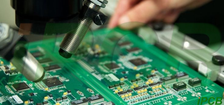
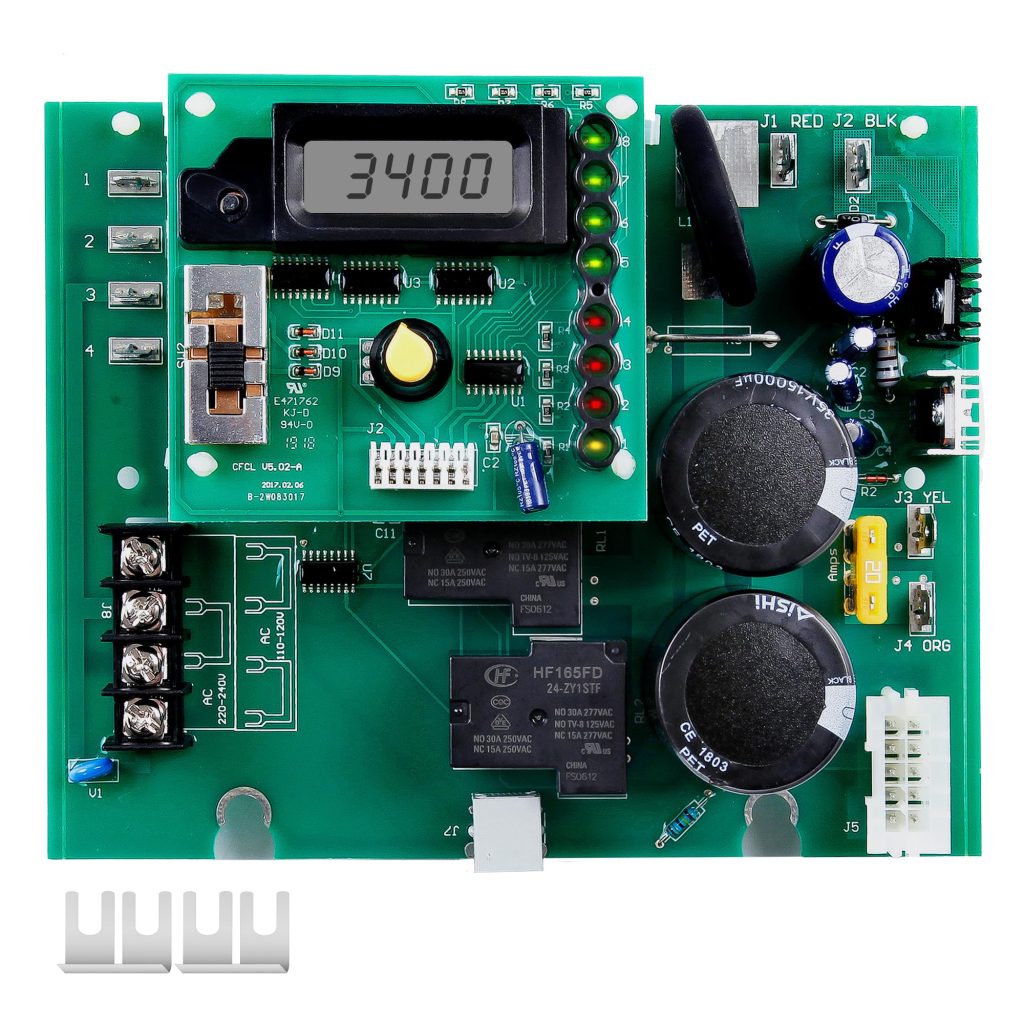
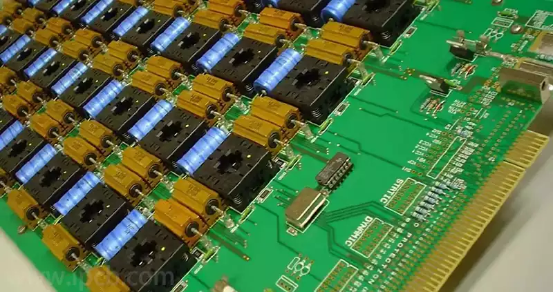
After etching, exposed copper conductors on a printed circuit board (PCB) will rapidly react electrochemically with oxygen and water molecules if directly exposed to the atmosphere, forming a thin film of copper oxide that cannot be easily removed by flux. This oxide not only destroys the copper layer’s good conductivity but also causes subsequent surface mount technology (SMT) and wave soldering to fail completely. To continuously protect the bare copper from oxidation during the months or even years from PCB manufacturing to final assembly and soldering, while providing an excellent soldering interface for component leads, surface treatment processes have emerged.
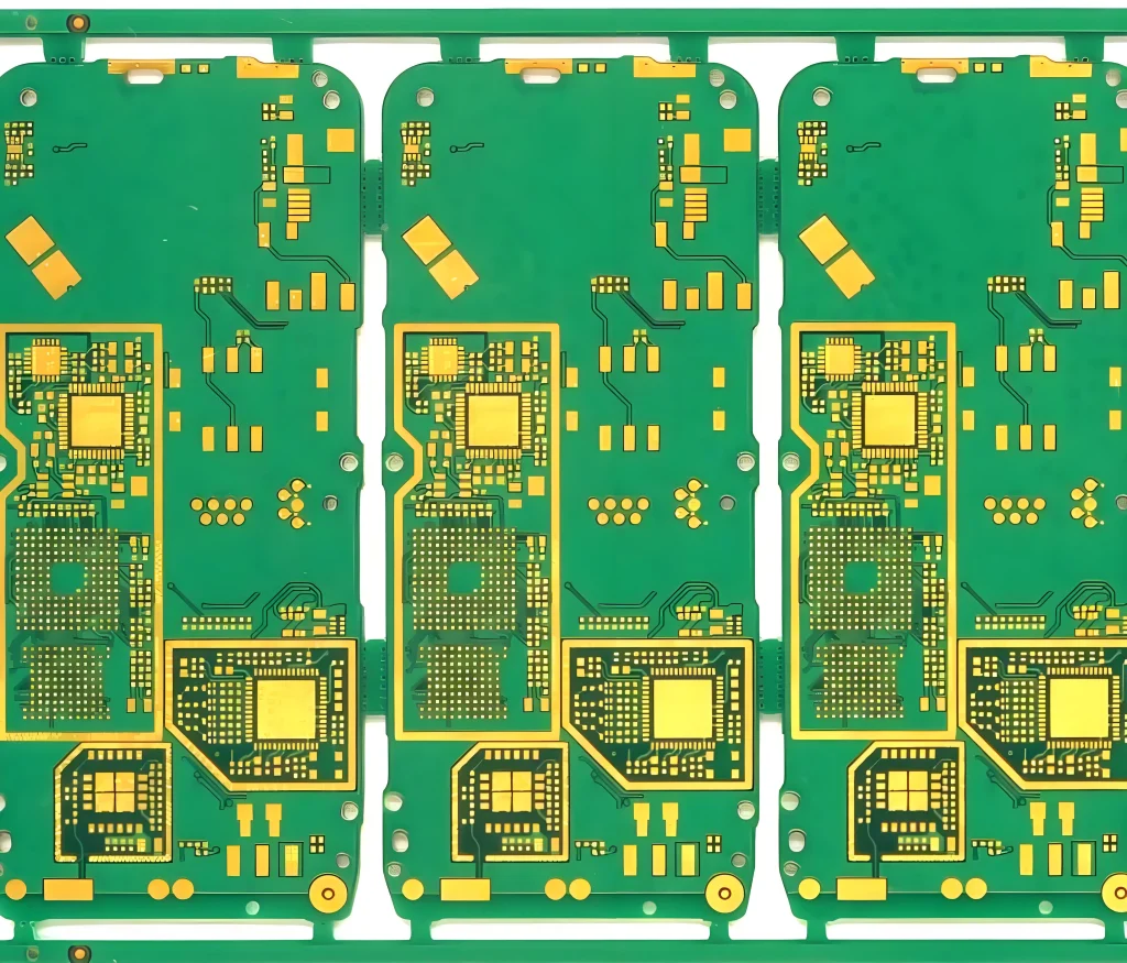
Among the many surface treatment technologies, Hot Air Solder Leveling (HASL) and Electroless Nickel Immersion Gold (ENIG) constitute two of the most representative technological pillars in modern electronics manufacturing. They represent not only two distinct philosophies of physicochemical protection but also represent a decades-long engineering evolution and competition across multiple dimensions, including micro-metallurgy, surface smoothness, production costs, and long-term reliability. Here is a article about comparative engineering analysis of HASL vs ENIG.
The Interplay of Melt Physics and Surface Tension: The Core Technology and Physical Limitations of HASL Process
Hot Air Leveling (HASL), one of the oldest and most mature surface treatment processes in the printed circuit board industry, is based on the core principles of pure molten metal wetting and fluid dynamics.
The Physical Processes of Soldering and Hot Air Scraping
In the HASL process, the circuit board, after pickling and micro-etching degreasing, is completely immersed in a molten solder bath at temperatures reaching 250°C to 260°C (in the lead-free era, this was typically a tin-silver-copper alloy or a tin-copper-nickel alloy). The molten solder instantly wets the exposed copper pads, and intense atomic diffusion occurs at the copper-tin interface, generating a micron-sized copper-tin intermetallic compound (IMC).
When the circuit board is pulled out of the molten solder bath at a fixed speed, two high-pressure jets of ultra-high-temperature compressed air (i.e., “hot air knives”) precisely blow onto both sides of the circuit board. High-pressure hot air not only powerfully removes residual solder from all metallized vias but also scrapes away excess liquid solder from the pad surface, leaving a uniform, bright solder coating with excellent solderability on the copper pad surface.
Meniscus Effect and Coplanarity Collapse
While the HASL process possesses inherent physical advantages in solder wettability and coating adhesion, fundamental principles of fluid mechanics also introduce fatal physical defects. When the molten solder cools and solidifies under the hot air, driven by surface tension, a pronounced “meniscus effect” forms at the pad edges.
This phenomenon causes the solder to bulge upwards in the center of the pad due to surface tension contraction, forming a dome-shaped microstructure that is thicker in the center and thinner at the edges. Even more critically, the solder thickness varies drastically across pads of different sizes: thicker solder remains on large power pads, while extremely thin solder remains on finely spaced signal pads.
As electronic components evolve towards miniaturization, micro-ball grid array (Micro-BGA), quad flat no-leads (QFN), and ultra-small surface-mount components such as 0201 and 01005 are widely used, placing extremely high demands on the surface coplanarity of the solder pads at the micrometer level. The bumps and uneven thickness introduced by HASL (Hyperplate Through-Hole) can cause physical tilting or suspension of microchip leads during placement. During subsequent reflow soldering, this coplanarity collapse can easily lead to bridging short circuits, cold solder joints, and “tombstone” failure due to uneven molten tension on both sides.
Thermal Stress Shock and Substrate Damage Besides surface unevenness, the HASL process, which involves directly immersing the entire circuit board in a high-temperature molten solder bath exceeding 250°C, represents a severe thermal shock to the PCB substrate. This instantaneous exposure to high temperatures causes the epoxy resin to expand dramatically, applying enormous tensile stress to the copper layer of the plated via (PTH) wall in the Z-axis direction. For complex multilayer boards with high layer counts and high aspect ratios, the thermal stress caused by HASL (High-Density Interconnect) can easily lead to inner layer copper foil breakage or copper layer pull-out and delamination on the via walls, creating hidden early fatigue failure risks for the circuit board.
Microscopic Creation of Autocatalytic and Displacement Reactions: The Chemical Precipitation and Physical Advantages of ENIG Process
When the coplanarity defects of HASL cannot meet the requirements of high-density interconnect (HDI) and ultra-fine pitch packaging, electroless nickel immersion gold (ENIG) has become a standard configuration for high-precision electronic products due to its superior flatness and highly controllable chemical precipitation mechanism.
Two-Stage Chemical Precipitation Mechanism
The ENIG process abandons the physical method of molten metal immersion coating, instead relying on precise electrochemical reactions to sequentially deposit two metal coatings with completely different functions on the copper surface:
Stage 1: Autocatalytic Electroless Nickel Plating
After activation with palladium colloid, the circuit board is immersed in an electroless nickel plating bath containing hypophosphite reducing agent. Under the action of a palladium catalyst, nickel ions in the solution are reduced and crystallized onto the copper surface, forming a nickel-phosphorus alloy layer typically 3 to 6 micrometers thick (phosphorus content is usually controlled at 7% to 9% in a medium-phosphorus system). This nickel layer is a true “functional barrier layer,” possessing extremely high physical hardness to effectively prevent copper atoms from diffusing to the outer layer, and also acting as an active nickel source for interfacial reactions during subsequent soldering.
Stage 2: Immersion Gold Plating After nickel plating, the circuit board is immersed in a gold salt solution. Because the electrode potential of nickel is significantly lower than that of gold, gold ions will strip electrons from nickel atoms in the solution, reducing them to free metallic gold, which is then deposited on the surface of the nickel layer. Simultaneously, the surface nickel atoms are oxidized and dissolved into the solution. This is a self-limiting displacement reaction; once the deposited gold layer completely covers the underlying nickel, blocking contact between nickel atoms and the gold solution, the displacement reaction automatically stops. The final gold layer is extremely thin, typically only 0.03 to 0.08 micrometers thick (i.e., 1.2 to 3.0 microinches).
Atomic-Level Flatness and High-Density Adaptability
Because ENIG relies entirely on the deposition and displacement of chemical molecules at a solid interface without an external electric field, its growth process strictly adheres to the geometry of the pad surface. Regardless of the pad size, from large power supply copper foil to tiny BGA micropads of tens of micrometers, the resulting nickel-gold coating thickness exhibits extremely high microscopic consistency.
This near-perfect atomic-level flatness allows ENIG to completely eliminate the meniscus effect of HASL, providing an absolutely flat physical base for the precise placement of ultra-fine pitch components. There is no leakage or missing prints during solder paste printing, and no slippage or tilting during chip placement, greatly improving the high yield and assembly reliability of high-density SMT components.
Multiple Reflow Soldering Compatibility and Contact Conductivity
Although the thin gold layer does not participate in the final soldering reaction (during reflow soldering, the gold layer quickly dissolves into the molten solder), it provides excellent oxidation protection for the underlying nickel layer. Even after multiple high-temperature reflow soldering cycles, the unsoldered ENIG pads retain their initial smoothness and activity. Furthermore, the extremely low contact resistance and excellent wear resistance of the gold layer allow the ENIG pads to directly function as button contacts, gold finger insertion/removal interfaces, and test probe contacts, achieving “multi-purpose” engineering integration.
In-depth Explanation of Interface Metallurgy: IMC Formation Mechanism and Black Pad Failure Mode Showdown
The core of evaluating surface treatment quality lies in the intermetallic compound (IMC) formed between the pads and solder at the high temperatures of reflow soldering. The microstructure and crystal structure of the IMC directly determine the tensile strength and shear resistance of the solder joint.
Differences in Physical Properties between Copper-Tin IMC and Nickel-Tin IMC
When soldering on HASL pads, the molten solder directly acts on the already formed copper-tin IMC (mainly a six-copper, five-tin phase). As the solder melts, copper atoms further diffuse into the solder, generating a uniform, continuous, and dense copper-tin intermetallic compound. This copper-tin IMC layer possesses excellent toughness and bonding strength, capable of withstanding severe mechanical vibration and thermal cycling stress.
However, soldering on ENIG pads is a much more complex process. After reflow soldering begins, the outermost gold layer rapidly dissolves and disperses into the solder within seconds (if the gold layer is too thick, the dissolved gold will form brittle gold-tin compounds during solder joint crystallization, leading to “gold embrittlement” failure). Subsequently, the tin in the molten solder undergoes a metallurgical reaction with the nickel in the substrate, forming nickel-tin intermetallic compounds (primarily trinickel-tetratin phase).
ENIG’s Nightmare: A Microscopic Analysis of the “Black Pad” Phenomenon
While ENIG provides perfect flatness, its unique electrochemical displacement mechanism also introduces one of the most fatal failure modes in electronic packaging—the “black pad” (also known as the black nickel phenomenon).
The root cause of the black pad occurs during the second-stage displacement gold plating process. If the chemical composition of the gold bath is unbalanced (e.g., too low pH, abnormal gold ion concentration, or too high reaction temperature), the displacement reaction rate will no longer be gentle, but will evolve into “hyper-corrosion” of the underlying nickel layer along the grain boundaries. Gold ions penetrate deep along the grain boundaries of the nickel-phosphorus alloy, frantically eroding and dissolving nickel atoms, while leaving needle-like or network-like microscopic gaps in situ.
Because nickel is selectively and massively dissolved, phosphorus elements originally bound to the nickel layer cannot be displaced and can only accumulate on the surface of the plating, forming a high-phosphorus amorphous transition layer (tri-nickel-phosphorus phase). When this damaged circuit board enters SMT reflow soldering, tin combines with nickel to form nickel-tin IMC, displacing a large amount of phosphorus below the IMC, causing this high-phosphorus brittle layer to thicken further.
The final solder interface is extremely fragile: the upper layer is nickel-tin IMC, and the lower layer is a damaged nickel layer with dense micro-pinholes and high-phosphorus enrichment areas, exhibiting a burnt black color. When equipment is subjected to drops, mechanical impacts, or thermal shock, the solder joints do not break from the solder itself, but rather peel cleanly away along the fragile “black pad” interface. This type of failure is highly insidious, often only manifesting itself suddenly after the product has been in use for some time, causing devastating damage to the product’s quality reputation.
In contrast, HASL, being a pure molten copper-tin physical coating, completely eliminates the electrochemical environment of displacement corrosion, thus being completely immune to the “black pad” failure hazard.
Manufacturing Window, Environmental Adaptability, and Economic Benefits: A Multi-Dimensional Trade-off
In actual industrial production, choosing between HASL and ENIG often requires finding the most rigorous engineering compromise among process control difficulty, production costs, shelf life, and environmental regulations.
Chemical Maintenance and Process Window Tolerance
HASL is a physically-dominated process. Its core factory management lies in the purity of the molten solder (preventing excessive copper contamination), the air pressure balance of the hot air knife, and the air temperature and lifting speed. While HASL equipment maintenance involves dealing with oxidation prevention and slag removal from high-temperature molten metal, its chemical system is relatively simple, with an extremely wide process window, requiring less expertise in microscopic chemical analysis from operators.
ENIG, on the other hand, is a highly sensitive microscopic chemical process. Its production line includes nearly ten complex chemical baths, such as acid degreasing, micro-etching, pre-dip, activation, electroless nickel plating, and immersion gold plating. The temperature, pH value, main salt concentration, reducing agent ratio, aging degree of organic additives, and accumulation of metallic impurities in each bath require real-time monitoring using high-precision titration analysis and ICP-OES spectrometry. Parameter drift in any process can lead to a surge in coating porosity, decreased adhesion, and even black pad disasters. Furthermore, ENIG wastewater contains large amounts of chelated nickel and heavy metals, making its wastewater treatment costs and environmental compliance requirements far higher than HASL.
Production Costs and Economic Feasibility
Cost structure is the most direct variable in the comparison between HASL and ENIG.
HASL (especially traditional leaded HASL): Low material cost, huge production capacity after initial equipment investment, and extremely low processing cost per unit area make it the preferred choice for low-to-mid-range consumer electronics and high-volume industrial control boards. Even when switching to lead-free HASL (LF-HASL), although the alloy cost increases due to the addition of silver, copper, or nickel, the overall economics are still significantly better than chemical gold plating.
ENIG: Due to the need to consume expensive precious metal gold salts, and the limited lifespan of the chemical nickel plating bath (usually requiring replacement after several cycles), coupled with high costs for chemical analysis and wastewater treatment, the processing cost of ENIG is typically several times that of HASL. For large-size, high-layer-count circuit boards, surface treatment costs can account for a very significant proportion of the overall board cost.
Storage Life and Environmental Tolerance
Regarding storage and usage environments, the two exhibit different physicochemical properties:
Storage Life: HASL pads are covered by a natural solder alloy. When stored in a dry environment at room temperature, its solder wettability can easily be maintained for over 12 months, demonstrating strong immunity to minor moisture and environmental contamination. While ENIG has a highly inert gold layer, its extremely thin layer and micropores mean that if stored for extended periods in harsh industrial air containing sulfides and chlorides, the underlying nickel will diffuse and oxidize along the micropores, forming difficult-to-remove nickel oxides. This leads to a significant decline in solder wettability after 6 to 12 months.
Moisture Resistance and Thermal Cycling: In extremely high humidity and salt spray environments, HASL’s thick solder layer provides a robust physical barrier to the underlying copper. However, if the porosity of the ENIG plating is not well controlled, it is prone to microscopic electrochemical bimetallic corrosion (Galvanic Corrosion) at the nickel-copper interface.
Selection Decision Topology: Modern Application Judgment of HASL vs ENIG
Faced with complex physical characteristics and manufacturing realities, engineering design teams should not blindly pursue high prices or traditional methods when selecting PCB surface treatments. Instead, they should base their decisions on a logical basis that includes clear component packaging forms, high-frequency electrical requirements, and product application scenarios.
Scenarios where HASL (or lead-free HASL) is preferred:
- Circuit boards with large pitch and through-hole mounting: Such as industrial switching power supplies, main control boards for home appliances, and high-current power distribution boxes in automobiles. The components in these products are mostly standard surface-mount (0805 and larger) or through-hole (DIP) devices, completely insensitive to surface coplanarity. HASL’s superior bonding strength, high cost-effectiveness, and high wettability make it the best solution.
- High-volume products with extremely sensitive costs: In the fiercely competitive low-end consumer electronics market, the cost per square centimeter determines the survival of a product. HASL offers a highly competitive manufacturing unit price.
- High-voltage electrical equipment requiring high-stress impact resistance: HASL’s robust copper-tin IMC interface better resists high mechanical stress and thermal vibration, preventing brittle fracture.
Scenarios where ENIG is preferred:
- High-density HDI and fine-pitch packaging: High-end smartphones, server motherboards, AI computing cards, etc., containing large-size micro BGAs (ball pitch less than 0.5 mm), QFN, CSP, or 0201/01005 micro passive components. ENIG’s extreme atomic-level flatness is a rigid prerequisite for ensuring high mounting yield and preventing bridging short circuits.
- Boards containing contacts and plug-in interfaces: Devices requiring onboard gold fingers, carbon film contacts for buttons, or pogo pins. ENIG’s wear-resistant and highly conductive gold layer can withstand multiple physical contact requirements.
- Complex double-sided SMT and multi-reflow soldering products: Complex multilayer boards requiring three or more high-temperature reflow soldering cycles. ENIG’s antioxidant protection ensures that the last soldered side still has perfect wetting activity.
- High-frequency microwave and radio frequency circuits: Although the nickel layer possesses ferromagnetism, introducing a slight “skin effect” loss for ultra-high frequency signals, the extremely flat physical geometry of ENIG remains crucial for precise parallel control of microstrip line impedance.
Through a microscopic analysis from melting physics to electrochemical precipitation, we can clearly see that HASL and ENIG are not simply substitutes, but rather two complementary camps evolved in the modern electronics industry to balance physical limits and commercial costs. The essence of engineering lies precisely in deeply understanding the fundamental differences between these two processes in micro-metallurgy, surface topology, and reliability models, thereby precisely matching the most perfect surface protection solution for each circuit board.