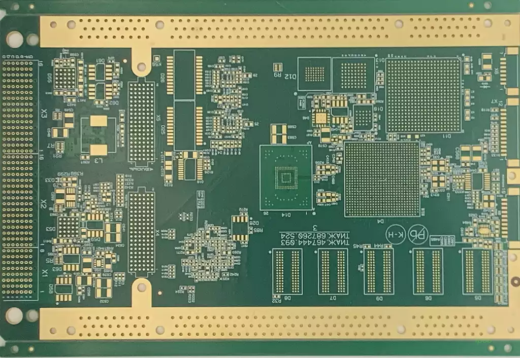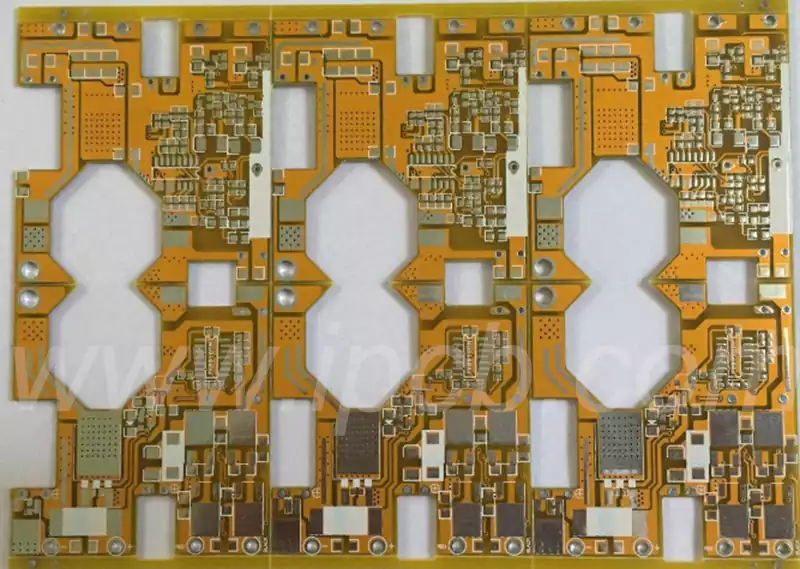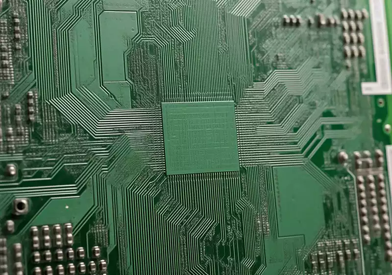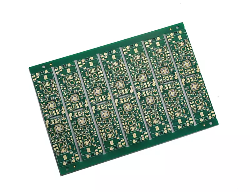
Printed circuit board dicing is a manufacturing process used to separate individual circuit boards from a larger production panel or substrate. During PCB fabrication and assembly, multiple boards are often arranged together in a single panel to improve material utilization, simplify handling, and increase production efficiency. After the required manufacturing or assembly operations are completed, the panel must be divided into individual boards with accurate dimensions and acceptable edge quality. The separation process needs to follow the designed board outline while protecting copper features, solder joints, components, and the internal structure of the PCB.
The choice of printed circuit board dicing method depends on the board material, thickness, outline geometry, production volume, and mechanical requirements. A simple rectangular board may be separated using a different process from a thin, densely populated circuit board with narrow connecting tabs or complex contours. Cutting accuracy is important, but it is not the only consideration. Excessive mechanical stress, dust, heat, or edge damage can affect the quality of the finished product. For this reason, dicing should be treated as an integral part of PCB manufacturing planning rather than an operation performed without considering the board design.
How Printed Circuit Board Dicing Works
Printed circuit board dicing begins with a panel design that defines how individual circuit boards are arranged and connected during production. The panel may contain multiple copies of the same design or several different board types. Small gaps, routing channels, V-grooves, or connecting tabs are incorporated into the panel according to the selected separation method. These features establish where the material will be removed or fractured when the boards are separated.
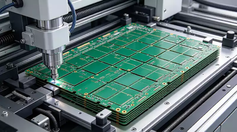
In a typical mechanical routing process, a rotating cutting tool follows a programmed path along the board outline. The cutter removes material from the panel and separates the individual PCBs. This approach is suitable for irregular shapes, curved edges, internal cutouts, and designs that cannot be separated using straight grooves. Tool diameter, cutting speed, feed rate, and fixture stability all influence the final result. Incorrect process settings may cause rough edges, excessive burrs, tool wear, or dimensional deviations.
V-cut separation uses a different principle. V-shaped grooves are machined into the top and bottom surfaces of the panel, leaving a controlled amount of material between the individual boards. The panel can then be separated along these weakened lines using appropriate equipment. This method is commonly used for boards with straight separation boundaries because it can support efficient panel processing. However, the remaining material must be carefully controlled. If the residual thickness is too large, separation may require excessive force; if it is too small, the panel may become fragile during handling.
Laser-based dicing uses a focused laser beam to remove or cut material along a defined path. It can support fine features and narrow cutting widths, making it useful for certain thin substrates and precision applications. The process does not rely on a conventional mechanical cutting blade, but thermal effects must still be considered. Depending on the material and laser parameters, heat-affected areas, discoloration, or changes to the cut edge may occur. Material compatibility and process validation are therefore essential.
Although these methods all separate circuit boards, they are not interchangeable in every application. The appropriate process must match the board construction, dimensional tolerances, edge requirements, and production conditions.
Choosing a Printed Circuit Board Dicing Method
Mechanical routing is often selected when a PCB has a complex outline or requires a clean separation path around curved sections and cutouts. Because the cutting tool follows a programmed route, manufacturers can accommodate different board shapes without relying on straight separation lines. However, the process introduces mechanical contact and cutting forces. Boards with fragile components, thin substrates, or sensitive structures may require additional support and careful fixture design.
V-cut separation is generally more suitable for panelized boards with straight edges. It can reduce the amount of material removed and support high-volume processing. Its limitations become apparent when a design contains curved outlines, protruding features, or components positioned too close to the separation boundary. The board layout must provide sufficient clearance for the V-groove and subsequent separation operation. Engineers should also consider the bending stress that can occur when the remaining material is broken apart.
Laser dicing may be considered when narrow cutting paths, small features, or specific material requirements make conventional mechanical separation less suitable. It can reduce mechanical contact with the board, but the equipment and process parameters must be matched to the substrate and copper structure. Laser wavelength, power, pulse characteristics, and scanning speed influence the cutting result. The method may also require additional consideration of debris removal and thermal effects.
Production volume is another factor in selecting a method. High-volume manufacturing may benefit from panel designs that allow fast and repeatable separation, while prototypes or low-volume production may prioritize flexibility and minimal tooling changes. The overall cost should include equipment setup, tooling wear, cycle time, material utilization, inspection, and the potential impact of damaged boards. A process that appears inexpensive at the cutting stage may become inefficient if it creates excessive rework or rejects.
Printed Circuit Board Dicing Design and Quality Control
Good dicing results begin with appropriate panel design. Engineers need to define separation lines, board spacing, tool access, and component clearance before the panel enters production. Components should not be placed too close to cutting paths because the separation operation may generate vibration, debris, or localized stress. Connectors, large components, fragile ceramic parts, and fine-pitch solder joints may require additional clearance depending on the cutting method.
The position of copper traces and internal structures also needs attention. Copper features close to the board edge may be exposed or damaged during cutting if the routing tolerance is not properly considered. Designers should establish suitable edge clearances and account for the actual cutting width, tool path deviation, and panel registration accuracy. For multilayer boards, the panel design must also protect internal copper structures and maintain the required insulation distance after separation.
Mechanical stress is a significant quality concern. Routing and V-cut separation can introduce vibration or bending forces that affect solder joints and components, particularly on densely assembled boards. Supporting the panel close to the cutting area can help reduce movement. The separation sequence should also be planned to avoid excessive stress on narrow connecting sections or partially separated boards.
Inspection verifies whether the process has produced boards that meet dimensional and appearance requirements. Measurements can confirm board length, width, outline position, and edge tolerances. Visual inspection can identify burrs, cracks, delamination, exposed copper, and other cutting defects. Where the application is sensitive to mechanical damage, additional inspection or functional testing may be needed after separation.
Process monitoring is equally important for repeatable production. Cutting tools should be checked for wear, equipment alignment should be maintained, and process parameters should be controlled. Changes in tool condition or fixture stability can gradually affect edge quality and dimensional consistency. For laser processes, monitoring beam conditions and cutting parameters helps maintain a stable result across production batches.
Improving Printed Circuit Board Dicing Reliability
A reliable printed circuit board dicing process depends on coordinating PCB design, panelization, equipment capability, and inspection requirements. The separation method should be selected according to the board’s material, thickness, shape, component layout, and required edge quality. Designers who consider dicing constraints early can reduce the risk of damaged components, rough edges, dimensional errors, and unnecessary manufacturing costs.
For complex or high-density boards, process validation is especially important. Trial cutting can help confirm whether the selected method produces acceptable edges and avoids damage to nearby circuitry. The results can then be used to refine panel spacing, cutting paths, tool settings, and support arrangements before full production begins. When these factors are controlled together, printed circuit board dicing becomes a predictable manufacturing operation that supports consistent board quality and efficient downstream assembly.