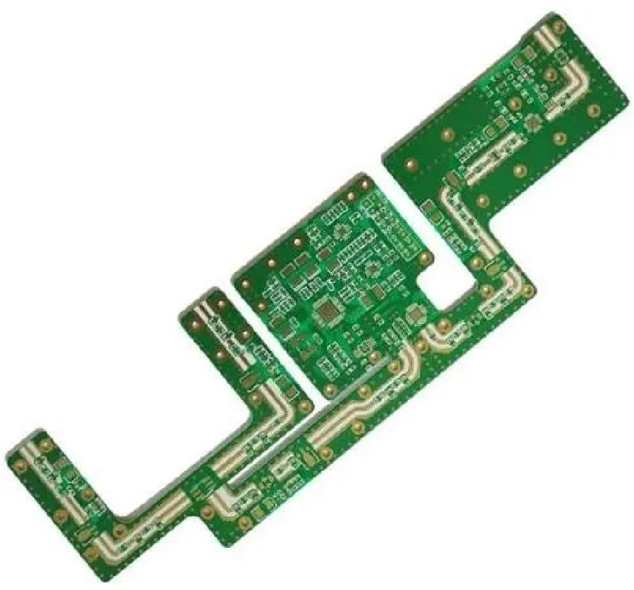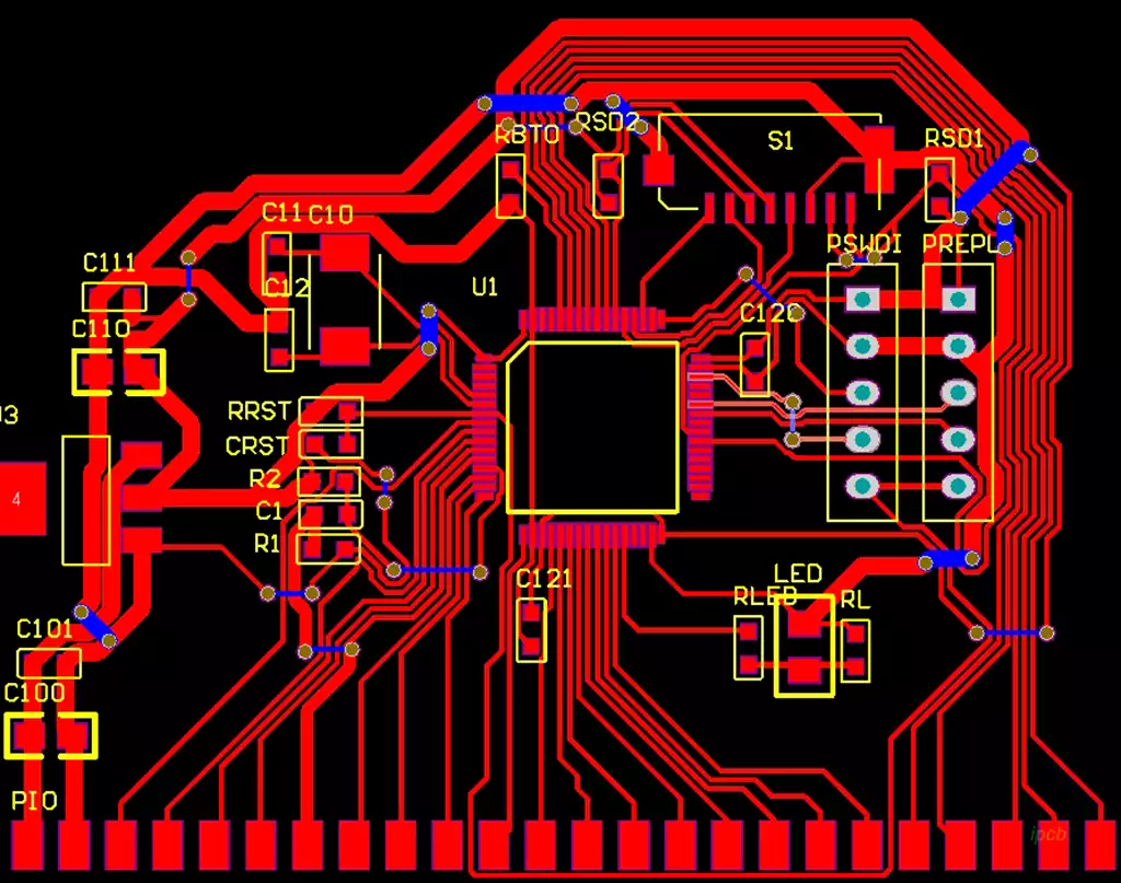
A multilayer rigid pcb aerospace solution must support electronic systems that operate under demanding electrical, thermal, and mechanical conditions. Aerospace equipment relies on electronic assemblies for navigation, communication, flight control, monitoring, power management, and data processing. These systems must maintain consistent performance despite vibration, temperature variation, limited installation space, and long operating periods. Multilayer rigid printed circuit boards provide a practical foundation for these applications by combining multiple copper layers within a mechanically stable insulating structure.
Unlike simpler circuit boards, aerospace PCBs often contain dense component layouts, complex signal paths, and multiple power and ground networks. A multilayer construction allows designers to distribute these electrical functions across dedicated copper layers while maintaining controlled spacing between conductive features. The rigid structure also provides a stable mounting platform for electronic components, connectors, and other assembly elements. However, achieving dependable performance requires more than increasing the layer count. Material properties, stackup design, copper distribution, fabrication precision, and verification procedures must all be considered as part of the engineering process.
Multilayer Rigid PCB Aerospace Applications and Structural Advantages
Aerospace electronic systems frequently combine digital processors, analog interfaces, RF circuits, sensors, and power electronics within relatively compact assemblies. Routing all these connections on one or two copper layers can become difficult as component density and circuit complexity increase. A multilayer PCB provides additional routing capacity and allows engineers to separate different electrical functions more effectively.
Ground and power planes are particularly important in these designs. A continuous ground reference can provide predictable return-current paths and help reduce electromagnetic interference. Dedicated power planes can distribute supply voltage across the board while reducing the need for numerous individual power traces. Signal layers can then be arranged around these reference structures to support controlled impedance and more consistent electrical behavior.
The rigid construction is equally significant. Aerospace assemblies may experience mechanical vibration, acceleration, and repeated temperature changes during operation. A rigid PCB provides structural support for components and helps maintain the physical relationships between solder joints, connectors, and conductive paths. Its mechanical properties depend on the substrate, copper configuration, board thickness, and overall laminate construction.
Space and weight limitations also influence PCB architecture. Designers may use higher layer counts to achieve dense routing within a smaller board area, although adding layers also increases manufacturing complexity and can affect overall thickness and weight. The goal is to develop a stackup that satisfies electrical and mechanical requirements without introducing unnecessary complexity.
Multilayer Rigid PCB Aerospace Materials and Layer Stackup
Material selection is a fundamental part of aerospace PCB development because the substrate affects electrical performance, dimensional stability, thermal behavior, and long-term reliability. FR-4 is widely used in electronic manufacturing, but not every FR-4 material is suitable for every aerospace application. Depending on operating frequency, temperature requirements, signal characteristics, and qualification criteria, engineers may need materials with specific dielectric, thermal, or mechanical properties.
The dielectric constant affects how electrical signals propagate through the board, while the dissipation factor influences dielectric losses. These characteristics become particularly important in high-speed digital and RF circuits. Material consistency is also important because variations in dielectric properties can affect impedance and signal timing. For designs with demanding high-frequency requirements, material selection should be based on actual electrical operating conditions rather than general material descriptions.
The layer stackup determines how copper and dielectric layers are arranged throughout the board. A carefully balanced stackup can improve mechanical stability, reduce warpage, and support predictable electrical performance. Designers need to consider copper thickness, dielectric spacing, core and prepreg selection, and the placement of power and ground planes. Symmetrical construction is often useful for controlling dimensional changes during lamination, although the final arrangement must also satisfy routing and electrical requirements.
Thermal properties deserve particular attention. Components in aerospace electronics may generate concentrated heat, especially in power conversion, processing, and communication circuits. The PCB must provide suitable thermal paths without compromising electrical isolation or signal performance. Copper planes, thermal vias, component placement, and appropriate substrate materials can all contribute to heat distribution. In applications with higher thermal loads, the board design may need to be coordinated with the enclosure and system-level cooling strategy.

Multilayer Rigid PCB Aerospace Electrical and Mechanical Design
Signal integrity is a major concern in multilayer aerospace circuit boards. High-speed signals can be affected by impedance discontinuities, crosstalk, reflections, and variations in return-current paths. These problems may result from unsuitable trace geometry, abrupt routing transitions, poorly positioned vias, or gaps in reference planes. Controlled-impedance routing and a well-planned stackup help reduce these risks.
Electromagnetic compatibility must also be addressed. Digital switching activity, RF transmission, and power conversion can introduce unwanted electromagnetic energy into nearby circuits. Separating sensitive analog or RF sections from noisy power and digital areas can help reduce coupling. Grounding strategy, shielding structures, filtering, and appropriate trace spacing should be considered together because no single layout technique can solve every interference problem.
Mechanical reliability depends on more than the rigidity of the substrate. Board edges, mounting holes, connector locations, component mass, and support points all influence how mechanical loads are transferred through the assembly. Heavy components may require additional mechanical support, while mounting arrangements should avoid concentrating stress around vulnerable areas. Copper distribution and board geometry should also be reviewed to reduce the risk of warpage during fabrication and assembly.
Thermal cycling can create stress because different materials expand and contract at different rates. This may affect plated through-holes, solder joints, laminate interfaces, and component connections. The board design should therefore consider the expected temperature range and the mechanical demands placed on critical structures. Where necessary, thermal and mechanical analysis can help identify areas that require additional attention before production.
Multilayer Rigid PCB Aerospace Manufacturing and Quality Control
Manufacturing a multilayer rigid PCB for aerospace applications requires consistent control over material preparation, inner-layer imaging, lamination, drilling, copper plating, outer-layer patterning, and surface finishing. Each process contributes to the quality of the final board. Defects such as internal shorts, open circuits, poor hole plating, insufficient insulation, and layer misregistration can affect electrical performance or long-term reliability.
Lamination is particularly important because multiple copper and dielectric layers must form a stable integrated structure. Inadequate bonding or unsuitable process conditions can lead to delamination, resin-related defects, or dimensional instability. Drilling and plating must also be controlled to ensure reliable electrical connections between layers. For designs with fine-pitch components or high routing density, registration accuracy and dimensional control become increasingly important.
Inspection and testing should reflect the complexity and intended use of the board. Automated optical inspection can identify visible pattern defects, while electrical testing checks for opens and shorts. X-ray inspection can help evaluate internal structures and selected assembly features. Depending on the application, additional testing may assess insulation resistance, dielectric withstand, thermal behavior, dimensional stability, and other specified requirements.
Aerospace projects may also require documented material traceability, controlled manufacturing processes, and formal qualification or acceptance procedures. The applicable requirements depend on the equipment, program, customer specifications, and relevant industry standards. Compliance should therefore be established during the design and procurement stages rather than assumed from the PCB layer count or material designation alone.
A reliable multilayer rigid pcb aerospace design is achieved when the board’s electrical architecture, material system, mechanical structure, and manufacturing process are developed as one integrated solution. The right combination of layer stackup, signal routing, thermal management, and quality controls allows complex electronic assemblies to operate consistently in demanding aerospace environments. For this reason, PCB development should begin with clearly defined application requirements and continue through engineering validation and controlled production.