The Microscopic World’s “Breakwater”: Electromagnetic Shielding
The Physical Essence of Multilayer Boards
In the macroscopic world of modern electronic design, various wireless communication technologies (such as 5G, Wi-Fi 6/7, Bluetooth, and GPS) enable our devices to seamlessly connect to the world. However, if we zoom out to the microscopic dimension inside the circuit board, it’s actually an extremely chaotic “electromagnetic free-for-all.”
When a high-density multilayer board begins to operate, the switching of transistors in the high-speed central processing unit (CPU), the high-frequency energy extraction from the switching power supply (DC-DC converter), and the radio transmission from the radio frequency amplifier (PA) all radiate chaotic and intertwined electromagnetic waves into the surrounding space. If these chaotic electromagnetic waves plunge into a delicate, weak signal receiving area (such as the front end of a GPS antenna or a high-precision analog amplifier), it will generate severe electromagnetic interference (EMI), causing intermittent mobile phone signals, GPS positioning failures, and even frequent system crashes due to data corruption.
To achieve “peaceful coexistence” on a tiny circuit board, engineers must build microscopic “electromagnetic dikes” between different functional areas—these are circuit board shields. Like metal lids, they firmly cover the most heat-generating “noise sources” or the most noise-sensitive “victims,” the chips, completely isolating them from different electromagnetic worlds.
The Duet of Absorption and Reflection: The Physical Extinguishing Mechanism of Electromagnetic Energy
The shields’ ability to block electromagnetic waves relies on two key defensive mechanisms of metallic materials: reflection loss and absorption loss.
When external electromagnetic waves rush towards the chip like ocean waves, they first strike the outer surface of the circuit board shields. Because the metal is filled with freely moving electrons, the moment an electromagnetic wave (essentially a changing electromagnetic field) touches the metal surface, high-frequency eddy currents are immediately induced. These eddy currents spontaneously generate a reverse electromagnetic field, like a mirror, “violently reflecting” the vast majority of the electromagnetic waves back. This is the first line of defense.
However, a small percentage of persistent high-frequency electromagnetic waves can still penetrate the metal surface and continue to infiltrate. At this point, the metal material’s second line of defense—absorption and loss—begins to function. As the electromagnetic waves penetrate the metal lattice, they continuously drive microscopic friction and agitation between atoms and electrons within the metal, silently converting the potentially destructive electromagnetic energy into weak heat energy, extinguishing it. Through this double interception, the electromagnetic conflict between the inside and outside of the cover is neutralized.
The Material Supply Chain’s Game of Interests: The Life-or-Death Choice Between Nickel Silver, Stainless Steel, and Aluminum Alloy
In the actual game of procurement and supply chain dynamics, the choice of material for circuit board shields directly determines the bare board price, surface mount yield, and long-term corrosion resistance. A precise balance must be struck among these three mainstream materials based on budget:
Nickel Silver (Copper-Nickel-Zinc Alloy):
This is the absolute king of high-end electronic products. Although it’s called “white copper,” it’s actually an alloy of copper, nickel, and zinc. Its greatest physical advantage lies in its excellent solderability and the fact that it requires no surface plating. Due to its high copper content, it can be directly and reliably soldered onto the PCB’s ground pads using solder paste during reflow soldering. Simultaneously, due to the presence of nickel, it is extremely resistant to rust in humid environments and possesses excellent magnetic permeability, providing unparalleled shielding against high-frequency noise. Its only drawback is its high cost; the material cost is several times that of ordinary metals.
Stainless Steel: This is a highly cost-effective option. Stainless steel is extremely hard, providing exceptional rigidity and resistance to deformation even with a thin layer, and its cost is extremely low. However, it has a fatal flaw in its manufacturing process: ordinary solder simply cannot adhere to stainless steel. To allow it to be soldered onto the circuit board, the PCB manufacturer must perform a secondary “full-on tin plating” or “nickel plating” treatment on the stainless steel surface. This not only increases processing costs, but also, if the PCB manufacturer’s plating quality is substandard, the plating will peel off under the high temperatures of reflow soldering, resulting in large-area cold solder joints and causing significant disruption to the production line.
Aluminum alloy: Aluminum alloys are very lightweight and have excellent thermal conductivity, making them ideal for high-power automotive modules that require both electromagnetic shielding and chip heat dissipation. However, aluminum alloys instantly form an extremely dense aluminum oxide film on their surface when exposed to air, rendering ordinary soldering irons and solder paste completely ineffective. Therefore, aluminum alloy shielding covers cannot be directly soldered onto PCBs; they can only be secured with mechanical screws, clips, or made into a detachable die-cast housing. This significantly limits its application in miniature smartphones and consumer electronics.
The Hell of Surface Mount Technology and the Cost Balance of Detachable Two-Piece Designs
Having clarified the material properties, we must turn our attention to the automated surface mount technology (SMT) production lines in foundries (EMS). The mechanical structure design of the shielding cover directly determines whether this production line is a high-speed success or a rework disaster for the entire factory.
The “Blind Box” Soldering Disaster of One-Piece Shielding Covers
In the most primitive, low-cost designs, many hardware engineers, to save a few cents on mold costs, preferred to use “one-piece” shielding covers. This is simply a small metal box cover. During automated surface mount technology (SMT), the pick-and-place machine uses a nozzle to grab it and directly place it onto the PCB pads coated with solder paste. The entire board then enters a 260-degree Celsius high-temperature reflow oven for melting and soldering.
While this design has extremely low material costs, it becomes a huge “yield black hole” in industrial mass production.
Because when this metal cover passes through the reflow oven closed, the small chips, resistors, and capacitors inside are all tightly sealed in a dark, enclosed space. Due to extremely poor thermal convection inside the cover, it often happens that one end of a small capacitor melts while the other end is not fully heated, leading to numerous “tombstone” or “cold solder joint” defects.
Worse still, once the circuit board emerges from the furnace, the Automated Optical Inspection (AOI) camera on the production line lacks X-ray vision, making it impossible to see whether the components inside the cover are properly soldered. This becomes a pure “technical blind box.” Only when the final Functional Testing (FCT) reveals the board’s malfunction does the workers realize the internal short circuit. At this point, repair workers have to use high-powered hot air guns to frantically heat the shielding cover and painstakingly pry it off for rework. This not only easily damages the surrounding delicate traces and chips but also drives up the foundry’s labor costs to record highs.
Two-piece Structure: Eliminating Hidden Production Costs with a Two-in-One Approach
To completely eliminate the rework pitfall of “soldering blind boxes,” modern mainstream circuit board shields have been upgraded to a “two-piece” split structure.
This design is ingenious, dividing the shielding cover into two independent components: the shielding frame and the shielding cover.
In the SMT placement stage, the pick-and-place machine only needs to solder the topless, completely open “metal frame.” Because the interior of the frame is 100% exposed, the hot air from the reflow oven can blow evenly and without obstruction onto every internal pad, completely eliminating the problem of cold solder joints caused by internal temperature differences. After the circuit board exits the oven, AOI cameras and human eyes can clearly and thoroughly inspect the soldering quality of every micro-component inside.
Only after all functional and visual inspections have passed with high scores, confirming the entire board is flawless, will a worker or automated robot, much like a Lock & Lock lunchbox, easily snap the solid metal top cover onto the metal frame with a “click.”
This two-piece design not only dramatically increases production first-pass yield but also greatly facilitates after-sales maintenance. If a customer’s product has been used for several years and an internal chip fails, maintenance personnel can simply use small tweezers to gently pry open the top cover, directly replace the chip, repair it, and then replace the cover again. Mia, when negotiating with overseas teams, you must use this “Lifetime Cost (LCC)” logic to persuade them. While the initial mold cost for a two-piece design is slightly higher, the savings in rework costs and reputational damage during mass production are enough to allow them to recoup dozens of times their initial investment.
The Art of Microscopic Leakage and Venting: A Deep Defense Line of Design for Manufacturability (DFM)
A qualified electromagnetic shield is definitely not as simple as just drawing a solid iron box and sticking it onto a board. Under the scrutiny of micro-nanoscale processes, the design of the shield hides numerous microscopic physical pitfalls related to aerodynamics and fluid dynamics.
Balancing Heat Dissipation and Pressure: Why Must the Shield Be Covered with “Honeycomb”?
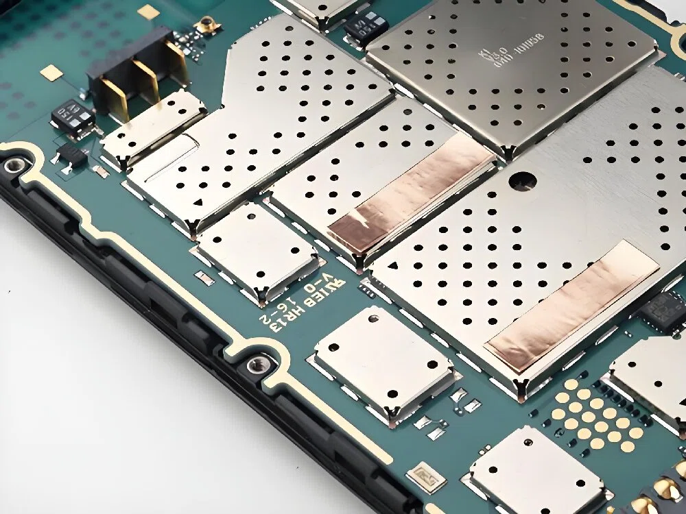
If you carefully observe the circuit board shields inside high-end servers or mobile phones, you’ll find that their tops are often not smooth planes, but neatly covered with densely packed small round holes, looking like a miniature honeycomb. These small holes are not just for aesthetics; they bear the dual physical mission of heat dissipation and pressure balance.
First, there is the vertical dissipation of heat. The components shielded are often high-heat-generating devices like main control chips or MOSFETs. If made into a completely sealed metal box, the interior would become a miniature thermos, with heat accumulating uncontrollably and causing the chip to overheat, triggering frequency reduction protection or even burning out within minutes. Numerous small holes allow the hot air inside to dissipate rapidly through convection, and combined with the thermal pads on top, the heat is directly transferred to the metal casing.
Secondly, it prevents the “rocket launch” effect during reflow soldering. In one-piece shielding or certain processes where capping is necessary during the surface mount stage, if the box is completely sealed, when the circuit board enters the reflow oven and the temperature suddenly jumps from room temperature to 260 degrees Celsius, according to the ideal gas law, the residual air inside the shield will undergo violent thermal expansion.
If the gas cannot find an outlet, the internal pressure will surge instantly, and the resulting upward thrust can push the thin metal shield open, shift, or even launch it like a small rocket into the oven, causing a large-scale shutdown of the entire production line. The numerous venting holes at the top provide a clear escape route for expanding gases, ensuring the shield remains stable on the solder pads even at high temperatures.
The Physical Game Between Aperture Diameter and Wavelength: How Big Should the Aperture Be to Prevent Light Leakage?
Given the many advantages of venting, can we make the holes infinitely large, or even create massive skylights?
The diameter of the hole must be much smaller than one-tenth of the wavelength of the electromagnetic wave being shielded.
Electromagnetic waves exhibit wave-particle duality. If the diameter of the venting holes on the shield exceeds a certain critical value for the electromagnetic wave wavelength, the hole ceases to be an obstacle in the eyes of the electromagnetic wave; instead, it becomes a free-flowing “supergate,” allowing high-frequency noise to escape without loss.
For example, suppose the customer’s board is processing a 5.8 GHz ultra-high frequency Wi-Fi signal. Physically, this signal has a wavelength of approximately 51 millimeters in air. To ensure that electromagnetic waves of this frequency cannot escape from the shield, the maximum diameter of the exhaust vents must be strictly limited to less than one-tenth of the wavelength (i.e., less than 5 mm). In practical high-reliability engineering, to achieve a reliable shielding effectiveness (greater than 40 dB), we typically lock the aperture between 1 mm and 1.5 mm. This size provides a perfect channel for air convection while physically creating a “nanoscale wire mesh” that electromagnetic waves absolutely cannot cross.
Creep Distance and Edge Interlocking: The Last Mile to Prevent Catastrophic Internal Short Circuits
Having completed the macro-planning of materials and structure, the final chapter of this article will delve into the details that drive field process engineers (PEs) crazy—the clearance between the inner wall of the shield and the components.
Shaking Metal Walls: Sudden Short Circuits Under Physical Vibration
In the extremely crowded PCB wiring areas of smartphones, drones, or the interior of a car’s center console constantly subjected to severe vibrations, the side walls of the shield are typically only a few tenths of a millimeter away from the internal surface-mount resistors and capacitors. Many junior designers, when designing circuit boards, consider the job done once they see “the sidewalls aren’t pressing against component pads” in the software. However, they completely overlook the three-dimensional deformation tolerances inherent in mechanical manufacturing.
Metal shielding is formed by stamping and bending thin metal sheets using molds. The bending process inevitably introduces angular tolerances, causing the sidewalls to not be perfectly perpendicular at 90 degrees, but rather to have slight inward or outward tilts.
When the product is installed in a car, the constant vibrations and bumps from the vehicle on uneven roads cause the thin metal sidewalls to wobble slightly under mechanical stress. If the sidewall is too close to the charged pads of internal components (e.g., less than 0.3 mm), in a sudden, violent impact, the inner metal wall can slam directly against the capacitor pads of the internal power chip due to the swaying. This instantaneous metal contact can cause a massive short circuit to ground across the entire power rail, instantly burning out the entire motherboard.
Ultimate Pitfall Avoidance Guidelines: The Golden Rules of Geometric Design for High-Level Shielding
To completely eliminate this ticking time bomb for both production and clients, IPCB, during high-end project drawing reviews (DFM), will strongly promote the following golden rules of geometry, summarized from countless lessons learned in the industry:
Vertical Height (Z-axis) Safety Clearance: The vertical distance between the top surface of the inner wall of the shielding cover and the top surface of the tallest chip inside (usually the main control SoC or inductor) must be at least 0.3 mm of absolute clearance. This space is to allow room for any subsequent thermal conductive silicone pads that may be attached, and to prevent the delicate chip below from being directly crushed if the center of the shielding cover collapses under pressure.
Horizontal Direction (X-Y Axis) Insulation Boundaries: The horizontal physical distance between the inner edge of the shielding cover and any component pads or exposed copper traces carrying electrical signals must be greater than 0.4 mm. If space is truly limited, engineers must forcibly apply a thin layer of polyimide (Kapton) insulating tape, capable of withstanding temperatures up to 300 degrees Celsius, around the inner walls of the shield. By introducing this layer of physical insulation, even if the sidewalls undergo severe deformation and shrinkage due to external forces, a metal short circuit will never occur, nipping the hidden risks in the bud during the design phase.