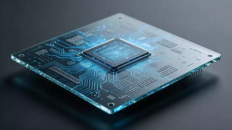
What is a glass substrate? Why has it become the core material for advanced packaging in the post-Moore’s Law era? Today, as the computing power of AI chips continues to rise and the number of transistors reaches the trillion-unit mark, traditional organic packaging substrates are approaching their physical limits in terms of transmission speed, wiring density and thermal stability, making it difficult to meet the demands of high-end AI computing power, high-speed interconnects and optoelectronic integration. The emergence of glass substrates is precisely intended to fill this technological gap.
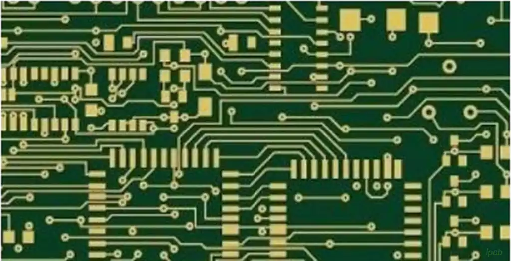
Many people tend to confuse glass substrates, PCBs and IC carrier boards. Put simply, a PCB board(printed circuit board) is the basic framework of an electronic device. Made from a composite of materials such as epoxy resin and glass fibre, it is low-cost and large in size, and is responsible for connecting the various components within the device. However, its trace widths are relatively thick, meaning it cannot directly package high-end chips. An IC carrier board, on the other hand, is an upgraded version of the PCB, acting as an interface between the bare chip and the PCB.
Currently, mainstream IC carrier boards are categorised into BT resin (balanced type, suitable for mobile phones and automotive applications) and ABF resin (high-precision, used for CPUs, GPUs and AI chips). Glass substrates, on the other hand, represent a brand-new advanced packaging substrate. Made from materials such as borosilicate glass and quartz glass, they utilise TGV (Through-Glass Via) technology to fabricate micrometre-scale vertical conductive channels, serving ultra-high-precision applications such as 2.5D/3D packaging and CPO (Chip-on-Optics) packaging.
To draw an analogy: if we compare an electronic system to a smart city, the PCB acts as the city’s main thoroughfares, responsible for connectivity between different areas; the IC carrier board is the internal roads within residential districts, precisely connecting the chip’s minute pins to the main thoroughfares; the glass substrate, meanwhile, is the underground high-speed utility tunnel—integrating ultra-high-density circuits within an extremely small space to achieve ultra-low-loss, ultra-high-speed data transmission, tailor-made for high-end computing chips.
It is important to note that glass substrates will not replace traditional PCBs, as they are highly brittle and cannot be manufactured in large sizes. Their aim is to replace high-end ABF and BT carrier boards, focusing on top-tier performance applications such as AI chip packaging, high-speed optical modules and RF devices.
Why are glass substrates so essential for AI chips? There are six key advantages:
1.Ultra-high interconnect density: For the same surface area, the interconnect density of a glass substrate is 10 times that of a traditional resin substrate, easily accommodating the interconnection requirements of trillions of transistors.
2.Extremely low signal loss: Glass has a low dielectric constant, resulting in minimal delay and low loss during high-frequency signal transmission, effectively preventing signal interference and lag during AI training and computation.
3.Nanometre-level flatness: With surface flatness at the nanometre level, line widths and spacings of less than 2 micrometres can be achieved, providing an ideal platform for high-precision lithography and packaging.
4.High-temperature resistance and stability: With a low coefficient of thermal expansion, the substrate does not warp or deform under high-temperature packaging or heavy loads, significantly improving packaging yield and long-term reliability.
5.Cost Reduction through Large-Panel Mass Production: Supports large-scale processing of 510×515mm ultra-large panels, enabling the packaging of multiple chips in a single process. This reduces costs by approximately 24% compared to traditional through-silicon via (TSV) processes, whilst eliminating the need for additional insulation layer deposition.
6.Natural Optoelectronic Integration: Glass possesses excellent light transmission and light-guiding properties, making it the optimal substrate for future CPO (Co-Packaged Optoelectronics) applications. It enables the integration of electronic chips and optical components, unlocking next-generation high-speed computing technologies.
Leveraging these exceptional performance advantages, the application scenarios for glass substrates are focused on high-end precision electronics and computing power sectors, with core implementation scenarios covering four major areas.
1.AI accelerators and high-end CPU/GPU packaging are the core drivers of current industrial implementation; leading chip manufacturers such as NVIDIA and AMD have already incorporated glass substrates into their core technology roadmaps.
2.CPO (Co-Packaged Optoelectronics), which significantly shortens signal transmission paths through the integrated integration of optoelectronic components, is a core technology for next-generation high-speed interconnects.
3.Mini/Micro-LED display packaging, which, thanks to its nanometre-level flatness, resolves the precision challenges of mass transfer, thereby enhancing display quality and yield rates.
4.High-density HDD storage, which is compatible with HAMR (Heat-Assisted Magnetic Recording) technology, facilitating high-density and high-performance upgrades for storage devices.
The industry generally regards 2026 as the inaugural year for mass production of glass substrates, and global semiconductor giants have already launched a ‘glass substrate arms race’:
Intel is the most vigorous proponent; at CES 2026, it launched the first Xeon 6+ server processor utilising a glass core substrate, achieving commercial deployment, and has invested over US$1 billion in Arizona to expand production capacity.
TSMC formally established its CoPoS advanced packaging solution for glass substrates in Q1 2026, with pilot production lines rapidly coming online. The company plans to replace traditional silicon interposers with glass substrates and is collaborating with Corning to develop specialised glass.
Samsung Electro-Mechanics has completed the delivery of glass substrate samples compatible with Apple’s AI chips, with mass production scheduled for 2026. Concurrently, the company is implementing TGV technology across its HBM4 high-bandwidth memory products.
Furthermore, companies such as Apple, LG Innotek and Japan’s Rapidus are also accelerating their efforts in areas including in-house AI chip packaging, opto-electronic hybrid transmission and large-size glass panels.
The domestic glass substrate industry started somewhat later and has long relied on imported materials and equipment. However, driven by the rise of the advanced packaging industry, policy support and the demand for domestic substitution, it has achieved a breakthrough from scratch. Currently in the pilot and small-scale mass production stages, the industry is rapidly narrowing the gap with overseas giants, whilst the full-chain domestic production layout continues to improve.
Glass substrates are not intended to replace traditional PCBs, but rather serve as a core upgrade vehicle for high-end IC carrier boards and the advanced packaging sector, forming a precise complement to traditional materials. TGV (Through-Glass Via) technology is its core competitive advantage, whilst precision equipment and specialised glass materials represent the key bottlenecks to current breakthroughs.
With the arrival of the mass production inflection point in 2026, the global glass substrate industry is entering a period of rapid development. Benefiting from the explosive growth in AI computing power and technological innovation driven by the physical limits of chip manufacturing processes, glass substrates are becoming the new cornerstone for extending Moore’s Law and empowering the trillion-dollar AI chip industry.
In the long term, China’s glass substrate market is projected to exceed US$3.7 billion by 2035, with the supporting CPO optical module packaging substrate market growing at a compound annual growth rate of over 55%. As continuous technological breakthroughs are achieved across the entire domestic materials, equipment and manufacturing value chain, domestically produced glass substrates will accelerate the realisation of self-reliance and control. They will comprehensively empower core industries such as AI computing power, optoelectronic packaging and high-end displays, becoming a key growth driver in the global advanced packaging sector.