As an upgraded next-generation PCB interconnect technology, UHDI has comprehensively surpassed the process and performance limits of traditional HDI boards, precisely meeting the evolving demands of today’s high-speed electronics industry. The rapid deployment of 5G and 6G communications, the Internet of Things (IoT), High-Performance Computing (HPC), Artificial Intelligence, and high-end medical electronics is driving electronic packaging towards extreme miniaturisation, high density, high-frequency and high-speed performance, and high integration.
The routing precision and transmission performance of conventional HDI PCBs are no longer sufficient to meet the stringent standards of high-end applications. With core features such as ultra-fine trace widths, dense microvia interconnections and the integration of built-in passive components, UHDI technology has become the core solution for high-end precision circuit packaging, providing essential support for the evolution of high-precision electronic devices.
Core Structural Characteristics of UHDI
The performance advantages of UHDI stem from its proprietary thin-layer stacking structure design. Unlike the conventional lamination systems of traditional HDI, this technology strictly controls the thickness of the dielectric layers within the range of 10–15 μm. The ultra-thin dielectric layer structure significantly reduces microvia depth, with the maximum microvia depth controllable within 50 μm, enabling support for multiple sequential lamination and pressing processes, and allowing for repeated formation of multi-layer circuit stacks.
This structural design not only achieves ultra-high-density circuit interconnection layouts, resolving the challenge of low space utilisation in traditional boards, but also retains excellent mechanical stability, avoiding the defects of delamination and deformation common in thin-layer boards, thereby balancing precision with durability.
Leveraging its proprietary thin-layer structure and precision processes, UHDI has achieved three core upgrades: micron-level ultra-fine traces, high-density three-dimensional via interconnections, and the integration of passive components. These three characteristics complement one another, freeing PCB boards from the limitations of traditional layouts and demonstrating irreplaceable application value in miniaturised equipment, high-frequency transmission systems, and highly integrated hardware; they also form the core technological foundation of current high-end electronic packaging.
Material selection is the key factor determining UHDI’s high-frequency transmission performance, signal integrity and service life. The industry currently adopts low-Dk, low-Df specialty substrates as the core selection criteria, completely replacing traditional standard epoxy resin substrates to meet the demands of high-frequency, high-speed transmission scenarios.
In terms of dielectric performance parameters, UHDI-specific substrates have been precisely optimised. The dielectric constant (Dk) is stably controlled within the range of 2.7 to 3.2, effectively reducing signal propagation delay and ensuring the real-time nature of high-speed data transmission; the dissipation factor (Df) is below 0.002, minimising high-frequency signal transmission losses and eliminating signal attenuation and distortion issues.
Currently, mainstream materials suitable for UHDI mass production include ABF (Adhesive Bonded Film) from Ajinomoto, LCP (Liquid Crystal Polymer) and modified high-end epoxy resins. Thanks to their excellent insulation properties, low loss, flatness and conformability, these materials have become the core substrates for high-end UHDI circuit boards, comprehensively ensuring signal integrity under complex operating conditions.
To achieve UHDI ultra-fine pitch routing standards of 15μm or less, conventional-thickness copper foil cannot meet the process requirements; ultra-thin copper foil with a thickness of ≤5μm must be used. In ultra-fine routing processes, the surface flatness of the copper foil is a key indicator affecting high-frequency transmission efficiency and product yield, and is also a core focus of UHDI process control.
ED electrolytic copper foil is produced via an electrochemical deposition process. In a copper sulphate electrolyte, an electric field causes copper ions to deposit gradually onto the surface of a polished roller; the rotational speed of the roller directly determines the thickness of the copper foil—the slower the speed, the thicker the deposited copper layer. The surface of the copper foil in contact with the polishing roller can form an ultra-smooth structure with a surface roughness of Ra < 1 μm. This exceptionally smooth surface structure significantly optimises high-frequency transmission performance, making it the preferred copper foil material for high-frequency UHDI boards.
RA rolled and annealed copper foil, on the other hand, utilises a physical rolling process, in which copper ingots are repeatedly rolled through a rolling mill to produce ultra-thin copper foil, which is then softened through a high-temperature annealing process, significantly enhancing the foil’s ductility and flexibility. Thanks to its excellent bending performance, RA copper foil has become the core material of choice for flexible applications such as UHDI flexible circuit boards and precision wearable devices.
UHDI Micro-Vias and Via-Filling Processes
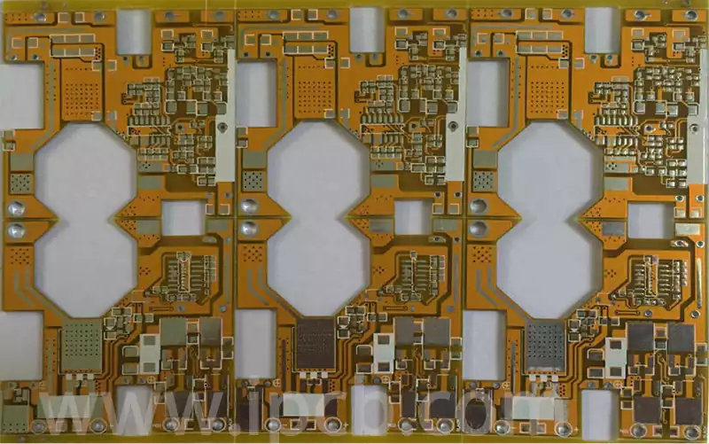
UHDI abandons the through-hole mechanical drilling structure of traditional PCBs, utilising blind vias and buried vias as the core interconnect structures to create a high-density three-dimensional routing system. Blind vias connect only the surface layer and the inner layers of the board; they open on one side and do not penetrate the entire board; buried vias are completely concealed between the board’s inner layers, with no contact with the outer board surface, thereby fully liberating surface routing space and significantly enhancing layout density.
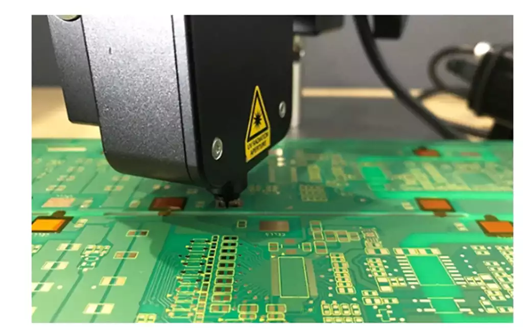
In terms of micro-via processing technology, laser drilling is the optimal solution for UHDI mass production, capable of precisely machining micro-vias within 50μm. Its precision and yield rates far exceed those of traditional mechanical drilling, whilst simultaneously avoiding defects such as chipping, misalignment and inconsistent hole diameters associated with mechanical drilling.
To balance ultra-high routing density with board structural reliability, UHDI boards commonly employ stacked or staggered micro-hole arrangements. Through scientific hole placement, stress is distributed to prevent the reduction in board strength caused by dense micro-holes, thereby achieving a balance between high-density interconnection and mechanical stability.
Via filling is a key process in UHDI precision manufacturing, which can further enhance board routing utilisation and optimise component assembly accuracy, whilst improving the circuit board’s electrical conductivity and thermal dissipation efficiency. It should be noted that the complexity of the via-filling process and the associated production costs are relatively high; consequently, the industry generally adheres to the principle of using it only where necessary, applying it exclusively in high-end precision applications.
Furthermore, the complementary application of pad-in-via technology can expand the effective contact area of the pads, improve the alignment accuracy and stability of the solder mask, and eliminate failure issues such as pad cracking and poor contact at the process source, thereby extending the product’s service life.
Based on the filling material and its conductive properties, UHDI microvia filling processes are categorised into conductive copper filling and non-conductive resin filling. Each process has its own advantages and disadvantages, and the appropriate selection must be made based on the product’s application scenario and performance requirements. Conductive filling uses pure copper as the filling medium, ensuring electrical continuity between stacked microvias whilst reinforcing the mechanical structural strength of the via locations.
Offering optimal stability and reliability, it is the mainstream choice for high-frequency and high-reliability applications. Copper filling allows for flexible application of various process solutions—such as electroplating-sealed filling, independent microvia filling, and simultaneous filling with through-holes—depending on electroplating equipment and chemical parameters, making it suitable for UHDI boards with different laminate structures.
Non-conductive filling utilises modified epoxy resin as the core material. Following filling, it requires electroplating levelling treatment to precisely control board thickness and flatness, providing a smooth and stable substrate for component mounting. This process is suitable for certain conventional precision applications.
However, its overall structural strength, electrical stability and high-temperature resistance are inferior to those of the copper-filled process, resulting in certain shortcomings in terms of reliability. Furthermore, epoxy resin filling must be carried out in a vacuum-sealed environment, which completely eliminates process defects such as residual bubbles and voids in the filling layer, ensuring uniform board quality.
Technical Advantages and Industry Prospects of UHDI
Through the innovative integration of five core technologies—ultra-thin dielectric layers, low-loss specialised substrates, ultra-fine precision copper foil, high-density stacked microvias, and embedded passive components—UHDI represents a comprehensive upgrade over traditional HDI PCBs. Compared to traditional processes, UHDI represents a qualitative leap in circuit interconnection density, high-frequency signal integrity and device integration, whilst offering more compact board dimensions and greater adaptability to operating conditions, perfectly aligning with the electronics industry’s trends towards miniaturisation, high-speed operation and high integration.
In cutting-edge fields such as 5G/6G communications, IoT smart terminals, high-performance computing equipment, artificial intelligence hardware and high-end medical electronics, UHDI has become a core, essential technology. As high-end electronic packaging technologies continue to evolve, and market demands for PCB precision, stability and transmission speeds continue to rise, UHDI’s material systems and laminate structure technologies will be continuously optimised. It will gradually become the mainstream standard for high-end precision PCB manufacturing, continuously empowering technological innovation and product upgrades within the electronics industry.