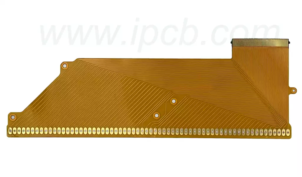
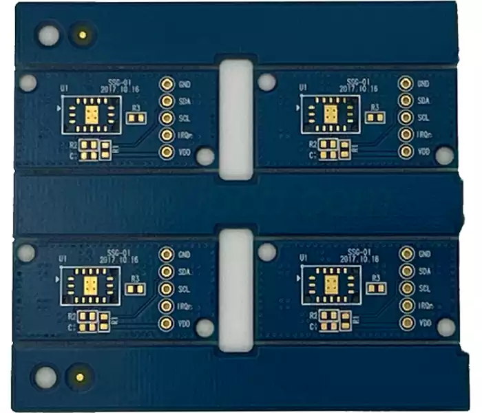
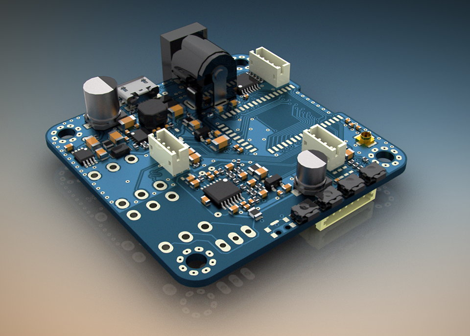
In printed circuit board (PCB) manufacturing, pcb warping and twists are often seen as the top defects in nonconformities, which often stems from a lack of in-depth understanding of their causes. Many novice inspectors incorrectly regard perfectly flat, rigid boards as the norm, but in reality, understanding the root causes of PCB warping and twisting is crucial to addressing these issues at the design stage.
Firstly, we need to clarify the difference between the terms ‘bow’ and ‘twist’. When all four corners of the board are in contact with the platform (imagine the shape of a bow), and the centre of the board lifts upwards, this is known as a ‘bow’ problem. Conversely, when only three corners are in contact with the platform and the fourth corner is raised, the problem is called ‘twisted’, and the IPC (International Powered Connectivity) has specific criteria for determining compliance in both cases.
So why does IPC allow a certain amount of warping or twisting? This is largely attributable to the materials and processes used in PCB manufacturing. PCB laminates are made up of multiple layers of glass fibre cloth and epoxy resin, each layer having its own unique thermal expansion properties. The thermal expansion properties of copper also need to be taken into account when adding copper layers to one or both sides of the laminate. During the manufacturing process, the board undergoes various etching and heat treatments that can cause the laminate to exhibit different reactions from sample to sample. As a result, IPC sets allowable tolerance ranges to account for normal manufacturing variations, even though manufacturers follow strict manufacturing processes.
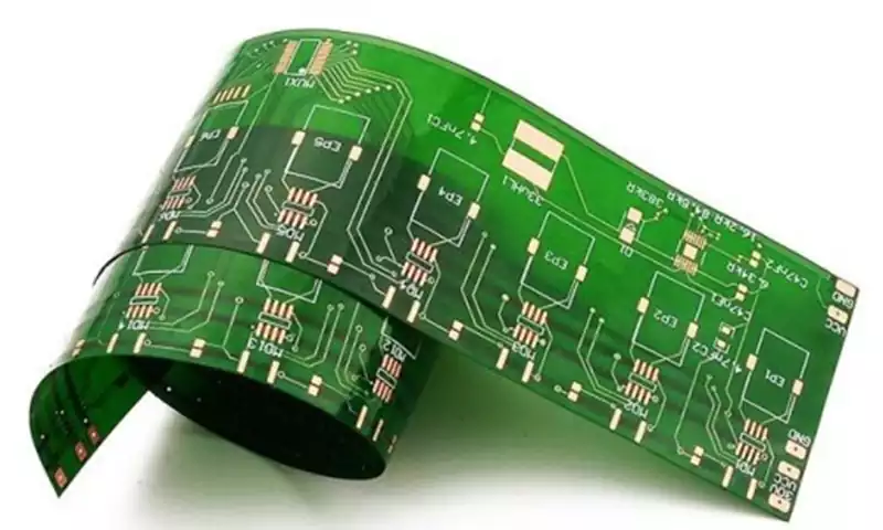
In addition to material and process factors,there are several other factors that can affect the degree of bowing and twisting of a PCB, including:
Addition of specific pcb component numbering features;
The addition of layers to the board (more material means more heat treatment);
Material mixing (e.g. using standard FR4 mixed with high frequency PTFE laminates to control impedance values, but can lead to unbalanced stacking);
Copper weight mixing (the high coefficient of thermal expansion of copper can negatively affect bowing and twisting).
In particular, when copper weights are unevenly distributed, high-density copper regions will expand into the region of least resistance under greater forces than low-density regions. Thus, balanced stacking (i.e., allowing layers with opposite thermal expansion values to interact with each other) is critical to maintaining uniform bowing and twisting forces. Unbalanced stacking, on the other hand, can result in the entire board being affected by the side with the greater thermal expansion value.
Additionally, the printed circuit board manufacturer needs to ensure proper storage of the raw laminate (to keep the material flat) and ongoing work handling (to prevent improper stacking of the production panels). In some cases, the manufacturer may also recommend reducing the amount of copper used in the design to reduce the risk of bending and twisting.
